An annular ring is the exposed copper area surrounding a hole on a printed circuit board (PCB), providing a reliable connection point for components, while a pad is the flat copper surface where components are soldered or mounted. Understanding the differences between annular rings and pads helps optimize Your PCB design for improved electrical performance and mechanical stability.
Table of Comparison
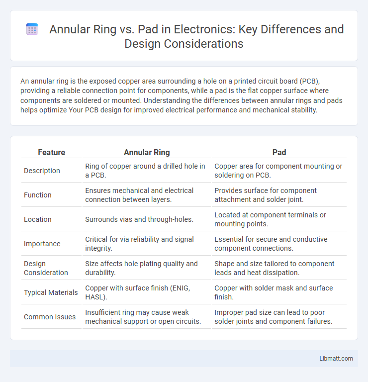
| Feature | Annular Ring | Pad |
|---|---|---|
| Description | Ring of copper around a drilled hole in a PCB. | Copper area for component mounting or soldering on PCB. |
| Function | Ensures mechanical and electrical connection between layers. | Provides surface for component attachment and solder joint. |
| Location | Surrounds vias and through-holes. | Located at component terminals or mounting points. |
| Importance | Critical for via reliability and signal integrity. | Essential for secure and conductive component connections. |
| Design Consideration | Size affects hole plating quality and durability. | Shape and size tailored to component leads and heat dissipation. |
| Typical Materials | Copper with surface finish (ENIG, HASL). | Copper with solder mask and surface finish. |
| Common Issues | Insufficient ring may cause weak mechanical support or open circuits. | Improper pad size can lead to poor solder joints and component failures. |
Introduction to Annular Rings and Pads
Annular rings are the conductive copper areas surrounding a drilled hole on a printed circuit board (PCB) that ensure reliable electrical connections between layers. Pads refer to the flat, exposed copper surfaces where components are soldered, providing mechanical support and electrical contact. Your PCB's signal integrity and component reliability depend on the precise design of both annular rings and pads.
What is an Annular Ring?
An annular ring is the copper area surrounding a drilled hole on a printed circuit board (PCB) pad, providing a reliable electrical connection and mechanical support for component leads or vias. It ensures signal integrity and durability by preventing pad damage during assembly or thermal cycling. Understanding the size and quality of the annular ring is crucial for optimizing your PCB design and manufacturing process.
What is a Pad in PCB Design?
A Pad in PCB design is a metal surface area used to connect electronic components to the circuit board, serving as a soldering point for component leads or surface-mount devices. Unlike the annular ring, which is the ring of copper around a drilled hole on a via or through-hole pad, the pad itself defines the exact area for component placement and soldering. Proper pad design ensures reliable electrical connection and mechanical stability while accommodating component lead dimensions and soldering requirements.
Key Differences Between Annular Rings and Pads
Annular rings are the exposed copper rings surrounding a drilled hole in a PCB, providing the electrical connection between the hole plating and the copper trace, while pads are the flat copper areas where components are soldered onto the board. The size and shape of annular rings directly impact the mechanical strength and electrical reliability of plated through-holes, whereas pad design primarily affects solder joint quality and component placement. Understanding these differences is crucial for PCB design optimization, ensuring proper electrical connectivity and mechanical stability.
Importance of Annular Rings in PCB Manufacturing
Annular rings are crucial in PCB manufacturing because they provide a reliable copper area around drilled holes to ensure strong electrical connections and mechanical stability between layers. A well-sized annular ring prevents issues like pad breakout or signal failure, which can compromise the durability and performance of your circuit boards. Choosing the correct annular ring size optimizes solder joint quality and minimizes manufacturing defects during the PCB assembly process.
Role of Pads in PCB Assembly
Pads in PCB assembly serve as critical contact points for component soldering, ensuring mechanical stability and reliable electrical connections. Their precise design, including size and surface finish, directly affects solder joint quality, signal integrity, and overall board durability. Unlike annular rings that focus on via-hole connections, pads are specifically tailored for surface mount device placement and solderability optimization.
Annular Ring vs Pad: Electrical Performance
The annular ring, the ring of copper surrounding a drilled hole in a PCB pad, plays a crucial role in electrical performance by ensuring reliable electrical connections and reducing the risk of open circuits. Pads, the flat conductive areas on a PCB where components are soldered, directly influence signal integrity and current carrying capacity, but a properly sized annular ring enhances mechanical strength and minimizes signal loss. Your PCB design's electrical performance depends significantly on optimizing the annular ring size relative to the pad to balance durability with signal efficiency.
Design Guidelines for Annular Rings and Pads
Design guidelines for annular rings and pads emphasize maintaining adequate copper width around vias and component leads to ensure mechanical strength and reliable electrical connections. An annular ring should generally be at least 0.15 mm wider than the drill hole to prevent potential breakout during PCB manufacturing. For your PCB design, ensure pad sizes comply with IPC standards, balancing solderability with space constraints while accounting for thermal relief and solder mask clearance to optimize assembly quality.
Common Issues Related to Annular Rings and Pads
Common issues related to annular rings and pads include misalignment and insufficient copper plating, which can cause poor electrical connectivity and weakening of the PCB structure. Pad lifting and delamination occur frequently due to excessive thermal stress or mechanical force during assembly or rework. Ensuring proper annular ring size relative to drill holes and using high-quality materials can help mitigate these risks and maintain your PCB's reliability.
Best Practices for Optimizing Annular Rings and Pads
Optimizing annular rings and pads requires maintaining appropriate ring widths tailored to PCB layer thickness and hole sizes, typically between 0.3 to 0.5 mm, to ensure reliable solder joints and electrical connectivity. Using proper pad shapes, such as round or teardrop, reduces stress and improves manufacturability by minimizing solder bridging and enhancing mechanical strength. Consistent annular ring dimensions combined with optimized pad tooling tolerances help prevent issues like pad delamination and improve overall PCB yield and durability.
Annular ring vs Pad Infographic