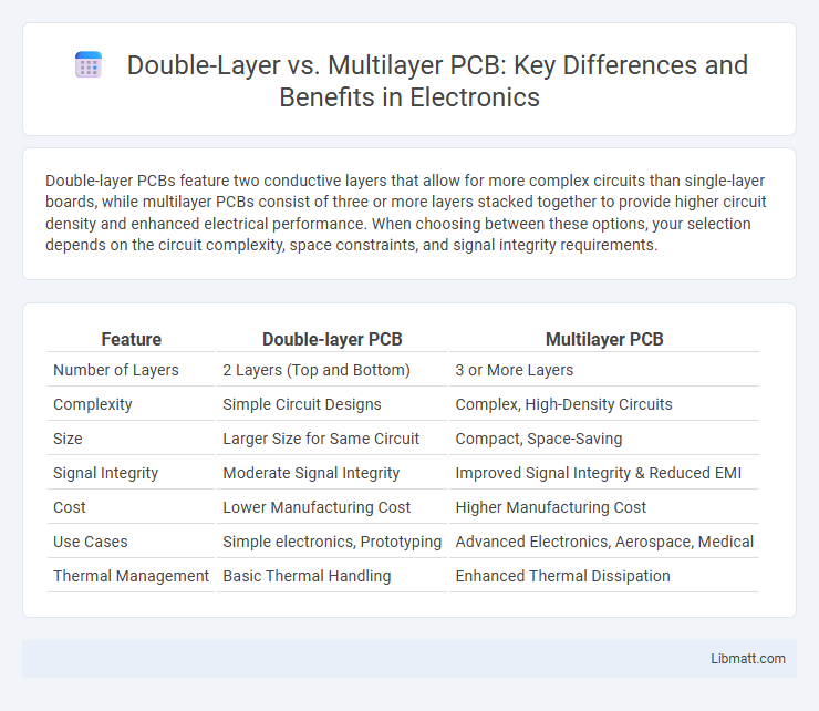
Double-layer PCBs feature two conductive layers that allow for more complex circuits than single-layer boards, while multilayer PCBs consist of three or more layers stacked together to provide higher circuit density and enhanced electrical performance. When choosing between these options, your selection depends on the circuit complexity, space constraints, and signal integrity requirements.
Table of Comparison
| Feature | Double-layer PCB | Multilayer PCB |
|---|---|---|
| Number of Layers | 2 Layers (Top and Bottom) | 3 or More Layers |
| Complexity | Simple Circuit Designs | Complex, High-Density Circuits |
| Size | Larger Size for Same Circuit | Compact, Space-Saving |
| Signal Integrity | Moderate Signal Integrity | Improved Signal Integrity & Reduced EMI |
| Cost | Lower Manufacturing Cost | Higher Manufacturing Cost |
| Use Cases | Simple electronics, Prototyping | Advanced Electronics, Aerospace, Medical |
| Thermal Management | Basic Thermal Handling | Enhanced Thermal Dissipation |
Introduction to PCB Layers
Double-layer PCBs consist of two conductive layers, typically one on the top and one on the bottom, allowing for more complex circuit designs compared to single-layer boards. Multilayer PCBs contain three or more layers of conductive material separated by insulating layers, enabling higher circuit density and improved electrical performance. Your choice between double-layer and multilayer PCB depends on the complexity, space constraints, and electrical requirements of your electronic project.
What is a Double-Layer PCB?
A Double-Layer PCB consists of two conductive copper layers separated by an insulating substrate, enabling complex circuit designs with components on both sides. This type of PCB supports higher component density and better electrical performance compared to single-layer boards, making it ideal for moderate complexity electronic devices. Double-layer PCBs enhance signal routing options and improve grounding and power distribution for reliable circuit functionality.
What is a Multilayer PCB?
A Multilayer PCB consists of three or more conductive layers separated by insulating materials, allowing complex circuit designs within a compact space. These layers are interconnected through vias, enabling high-density component placement and enhanced electrical performance. Multilayer PCBs are commonly used in advanced electronics such as computers, smartphones, and medical devices due to their space-saving and signal integrity benefits.
Key Differences Between Double-Layer and Multilayer PCBs
Double-layer PCBs consist of two conductive copper layers separated by an insulating layer, enabling simple and cost-effective circuit designs suitable for mid-complexity applications. Multilayer PCBs feature three or more layers, providing enhanced circuit density, improved signal integrity, and greater design flexibility for complex electronics like smartphones and aerospace systems. Key differences include manufacturing complexity, cost, signal interference management, and thermal performance, with multilayer PCBs excelling in high-density, high-speed, and high-reliability environments.
Advantages of Double-Layer PCBs
Double-layer PCBs offer a significant advantage in improved circuit density compared to single-layer boards, allowing for more complex designs within a compact space. They provide enhanced electrical performance through better signal integrity and reduced crosstalk due to the presence of a ground plane layer. Cost efficiency is another benefit, as double-layer PCBs are less expensive to manufacture and assemble than multilayer PCBs while still accommodating moderate complexity in electronic applications.
Advantages of Multilayer PCBs
Multilayer PCBs offer superior electrical performance and higher component density compared to double-layer PCBs, enabling complex circuit designs in compact spaces. Their enhanced signal integrity and reduced electromagnetic interference make them ideal for advanced electronics like smartphones and medical devices. The increased reliability and scalability of multilayer PCBs support modern high-speed and high-frequency applications effectively.
Limitations of Double-Layer PCBs
Double-layer PCBs face limitations in handling complex circuitry due to their restricted routing layers, which can lead to signal interference and increased crosstalk in high-density designs. Thermal management becomes challenging as heat dissipation is less efficient compared to multilayer PCBs, impacting overall device performance and reliability. When your project demands compact, high-speed circuits with robust electrical integrity, multilayer PCBs provide enhanced flexibility and superior signal routing capabilities.
Limitations of Multilayer PCBs
Multilayer PCBs face limitations such as increased manufacturing complexity and higher costs compared to double-layer PCBs, which can impact your project's budget and timeline. Signal interference and thermal management become more challenging as layer count increases, potentially affecting performance and reliability. Design constraints also arise from the difficulty in routing and testing dense multilayer configurations, requiring advanced tools and expertise.
Choosing the Right PCB: Application Considerations
Double-layer PCBs offer moderate circuit complexity with two conductive layers suitable for simpler electronic applications, while multilayer PCBs provide increased complexity and compactness by stacking multiple layers, ideal for advanced devices requiring high-density interconnections. Your choice depends on application factors such as signal integrity, electromagnetic interference control, size constraints, and cost efficiency. Evaluating these criteria ensures optimal performance and reliability tailored to your specific electronic design needs.
Summary: Double-Layer vs Multilayer PCB
Double-layer PCBs have two conductive layers separated by an insulating material, offering moderate complexity and cost-effectiveness preferred for simpler electronic circuits. Multilayer PCBs consist of three or more layers, providing higher circuit density, improved signal integrity, and enhanced performance for advanced devices and compact designs. Your choice depends on project requirements, balancing complexity, space constraints, and budget.
Double-layer vs Multilayer PCB Infographic