A Plated Through Hole (PTH) is a drilled hole in a PCB that is coated with conductive material to allow electrical connection between multiple layers and can also accommodate component leads. A Via is a smaller, typically non-component mounting hole used solely to connect different PCB layers internally, optimizing space and signal routing in your circuit design.
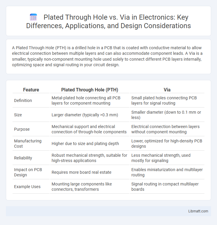
Table of Comparison
| Feature | Plated Through Hole (PTH) | Via |
|---|---|---|
| Definition | Metal-plated hole connecting all PCB layers for component mounting | Small plated holes connecting PCB layers for signal routing |
| Size | Larger diameter (typically >0.3 mm) | Smaller diameter (down to 0.1 mm or less) |
| Purpose | Mechanical support and electrical connection of through-hole components | Electrical connection between layers without component mounting |
| Manufacturing Cost | Higher due to size and plating depth | Lower, optimized for high-density PCB designs |
| Reliability | Robust mechanical strength, suitable for high-stress applications | Less mechanical strength, used mostly for signaling |
| Impact on PCB Design | Requires more board real estate | Enables miniaturization and multilayer routing |
| Example Uses | Mounting large components like connectors, transformers | Signal routing in compact multilayer boards |
Introduction to Plated Through Hole and Via
Plated Through Hole (PTH) refers to a hole in a printed circuit board (PCB) that is drilled through the entire board and coated with a conductive material to create an electrical connection between different layers. A Via is a smaller, more specialized PTH used exclusively for inter-layer connections in multi-layer PCBs, typically without component leads inserted. Both PTH and Vias play crucial roles in ensuring electrical continuity and signal integrity within complex PCB designs.
What Are Plated Through Holes (PTH)?
Plated Through Holes (PTH) are conductive holes drilled through a printed circuit board (PCB) and lined with metal to create electrical connections between different layers. Unlike vias, which are primarily used for signal routing, PTHs often serve as mounting points for component leads and stronger mechanical connections. Understanding the role of PTHs enhances your ability to design reliable, multi-layer PCBs with effective electrical and structural integrity.
Understanding PCB Vias
PCB vias are crucial for electrical connectivity, providing pathways between different layers of a printed circuit board. Plated through holes (PTH) are specific types of vias plated with conductive material to ensure reliable signal transmission and mechanical stability. Differentiating between via types such as through-hole, blind, and buried vias enhances PCB design optimization for signal integrity and manufacturing efficiency.
Key Differences Between PTH and Via
Plated Through Hole (PTH) and Via are both essential elements in PCB design but differ primarily in function and structure. PTHs are typically larger holes used for mounting and connecting components through the entire board, providing mechanical support and electrical connectivity. Vias are smaller holes mainly designed to electrically connect different layers of a multi-layer PCB without component insertion, optimizing space and signal routing.
Types of Vias in PCB Design
Plated Through Holes (PTH) and Vias serve distinct purposes in PCB design, with PTHs primarily used for component mounting and Vias for electrical connections across layers. The main types of vias include Through Vias, which pass through all PCB layers; Blind Vias, connecting outer layers to inner layers without going through the entire board; and Buried Vias, located entirely within inner layers, invisible from outer surfaces. Understanding these via types helps optimize your PCB for signal integrity, space constraints, and manufacturing costs.
Benefits of Plated Through Holes
Plated Through Holes (PTH) provide robust electrical connections by allowing components to be soldered directly, enhancing mechanical strength and reliability in multilayer PCBs. Their precise plating ensures consistent conductivity and thermal dissipation, which is critical for high-power applications. Your PCB designs benefit from increased durability and improved signal integrity when using Plated Through Holes over standard vias.
Applications of Vias in Modern Electronics
Vias are essential in modern electronics for creating multilayer printed circuit boards (PCBs) that enhance signal routing and electrical connectivity between different board layers. Their applications range from high-frequency communication devices to compact mobile gadgets, enabling efficient space utilization and improved circuit performance. Your PCB designs benefit significantly from vias when requiring robust electrical connections and optimized board layouts in complex electronic assemblies.
Manufacturing Processes: PTH vs Via
Plated Through Holes (PTH) are created by drilling holes through the entire PCB substrate followed by copper plating, providing strong mechanical support and reliable electrical connections for component leads. Vias, on the other hand, involve drilling smaller holes that are copper-plated to connect different layers within multi-layer PCBs without accommodating component leads, thus enhancing signal routing and density. Your choice between PTH and vias affects manufacturing complexity, cost, and the overall functionality of the circuit design.
Cost Considerations: PTH vs Via
Plated Through Holes (PTH) typically incur higher manufacturing costs due to the extensive drilling and plating processes required for through-hole component mounting, impacting overall PCB production expenses. Vias, being smaller and more numerous, offer cost efficiency by minimizing drilling complexity and material usage, especially in high-density multilayer boards. Choosing between PTH and vias depends on balancing functional requirements with budget constraints, where vias generally provide a more economical solution for signal routing and inter-layer connections.
Choosing Between Plated Through Hole and Via
Choosing between a plated through hole (PTH) and via depends on your PCB design requirements and electrical connectivity needs. PTHs are suitable for component mounting and robust mechanical connections, while vias primarily serve as electrical pathways between PCB layers, optimizing space. Your decision should balance signal integrity, mechanical strength, and manufacturing cost to ensure optimal PCB performance.
Plated Through Hole vs Via Infographic