Solder mask provides a protective layer over the PCB to prevent solder bridges and corrosion, while paste mask, or solder paste stencil, guides the precise application of solder paste on pads before component placement. Understanding the difference enhances your PCB assembly accuracy and reliability.
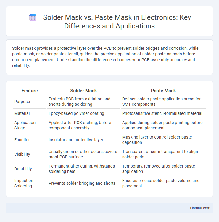
Table of Comparison
| Feature | Solder Mask | Paste Mask |
|---|---|---|
| Purpose | Protects PCB from oxidation and shorts during soldering | Defines solder paste application areas for SMT components |
| Material | Epoxy-based polymer coating | Photosensitive stencil-formulated material |
| Application Stage | Applied after PCB etching, before component assembly | Applied during solder paste printing before component placement |
| Function | Insulator and protective layer | Masking layer to control solder paste deposition |
| Visibility | Usually green or other colors, covers most PCB surface | Transparent or semi-transparent to align solder pads |
| Durability | Permanent after curing, withstands soldering heat | Temporary, removed after solder paste application |
| Impact on Soldering | Prevents solder bridging and shorts | Ensures precise solder paste volume and placement |
Understanding Solder Mask: Definition and Purpose
Solder mask is a protective layer applied to printed circuit boards (PCBs) that prevents solder bridges and oxidation during the soldering process, ensuring precise electrical connections and enhancing durability. Unlike paste mask, which is used to apply solder paste accurately to pads, solder mask covers the entire PCB except for the areas where soldering is required. Understanding solder mask helps you maintain the integrity of your PCB design by minimizing short circuits and improving overall reliability in electronic assemblies.
What is Paste Mask? An Overview
Paste mask, also known as solder paste stencil, is a thin layer of material applied to a printed circuit board (PCB) to define areas where solder paste will be deposited for surface mount component placement. Unlike solder mask, which protects the PCB from oxidation and prevents solder bridges, paste mask specifically guides the precise application of solder paste during assembly. Understanding paste mask is crucial for ensuring accurate solder joint formation and optimal electrical connections in your PCB manufacturing process.
Key Differences Between Solder Mask and Paste Mask
Solder mask protects exposed copper traces on a printed circuit board (PCB) by preventing oxidation and solder bridging during assembly, while paste mask defines areas for precise solder paste application on pads before component placement. The solder mask is typically a durable epoxy layer applied over the entire board except for pads, while the paste mask is a stencil-like layer used only during the solder paste printing process. These distinct functions optimize PCB assembly quality, with solder mask ensuring long-term electrical isolation and paste mask enabling accurate solder volume control for surface-mount devices.
Materials Used in Solder Masks vs Paste Masks
Solder masks primarily use epoxy-based polymers or liquid photoimageable materials designed to protect copper circuitry from oxidation and prevent solder bridging during PCB assembly. Paste masks, on the other hand, utilize solder paste composed of powdered metal (typically tin, silver, and copper alloys) mixed with flux, serving as a temporary adhesive for surface mount components before reflow soldering. Your choice depends on the mask's role; solder masks safeguard and insulate, while paste masks facilitate precise component placement and secure solder joints.
Application Processes: Solder Mask vs Paste Mask
Solder mask is applied using a liquid photoimageable process that involves coating the PCB surface, curing, and then exposing it to UV light through a photomask to create protective layers over copper traces. Paste mask, commonly known as solder paste stencil application, involves applying a stencil over the PCB and depositing solder paste precisely onto pads where components will be soldered. Understanding these distinct application processes helps optimize your PCB manufacturing workflow by ensuring accurate protection and soldering readiness.
Role of Solder Mask in PCB Manufacturing
The solder mask in PCB manufacturing serves as an insulating layer that protects copper traces from oxidation and prevents solder bridging during component assembly, ensuring electrical isolation and enhancing circuit reliability. It defines precise areas on the PCB where solder paste should not be applied, thereby facilitating accurate solder paste application and improving the overall assembly process. By controlling soldering regions and protecting the board from environmental contaminants, the solder mask significantly contributes to reducing defects and increasing the longevity of electronic components.
Importance of Paste Mask in Surface Mount Technology
Paste mask plays a crucial role in Surface Mount Technology by precisely controlling the application of solder paste on PCB pads, ensuring accurate component placement and reliable electrical connections. Unlike solder mask, which primarily protects the board from oxidation and short circuits, paste mask directly impacts solder joint quality and assembly yield. Your manufacturing process benefits significantly from consistent paste deposition, reducing defects and improving overall production efficiency.
Common Issues and Defects: Solder Mask vs Paste Mask
Common issues with solder mask include delamination, pinholes, and improper coverage, which can lead to solder bridging and corrosion. Paste mask defects often involve misalignment, incomplete stencil openings, and inconsistent thickness, resulting in insufficient or excessive solder paste deposition. Both masks require precise application and curing processes to ensure reliable solder joint quality and avoid component placement failures.
Design Considerations for Solder Mask and Paste Mask
Design considerations for solder mask include precise alignment to prevent solder bridging and ensure circuit protection, with emphasis on appropriate clearance around pads and traces to optimize electrical insulation and mechanical durability. For paste mask, design must focus on accurate aperture sizing and positioning to achieve consistent solder paste deposition, directly impacting solder joint reliability and component placement accuracy. Both masks require careful coordination to avoid overlap issues, ensuring robust PCB assembly and optimal manufacturing yield.
Tips for Choosing Between Solder Mask and Paste Mask
Selecting between solder mask and paste mask depends on the specific PCB manufacturing requirements and the desired level of protection against oxidation and solder bridging. Solder mask is ideal for protecting copper traces and preventing short circuits, while paste mask is essential for accurately applying solder paste to pads during assembly. Evaluate the PCB design complexity, component density, and manufacturing process to determine the most suitable mask type for optimal soldering quality and reliability.
Solder Mask vs Paste Mask Infographic