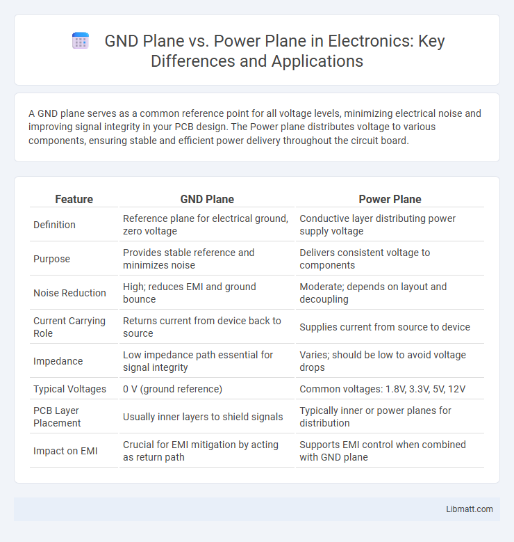
A GND plane serves as a common reference point for all voltage levels, minimizing electrical noise and improving signal integrity in your PCB design. The Power plane distributes voltage to various components, ensuring stable and efficient power delivery throughout the circuit board.
Table of Comparison
| Feature | GND Plane | Power Plane |
|---|---|---|
| Definition | Reference plane for electrical ground, zero voltage | Conductive layer distributing power supply voltage |
| Purpose | Provides stable reference and minimizes noise | Delivers consistent voltage to components |
| Noise Reduction | High; reduces EMI and ground bounce | Moderate; depends on layout and decoupling |
| Current Carrying Role | Returns current from device back to source | Supplies current from source to device |
| Impedance | Low impedance path essential for signal integrity | Varies; should be low to avoid voltage drops |
| Typical Voltages | 0 V (ground reference) | Common voltages: 1.8V, 3.3V, 5V, 12V |
| PCB Layer Placement | Usually inner layers to shield signals | Typically inner or power planes for distribution |
| Impact on EMI | Crucial for EMI mitigation by acting as return path | Supports EMI control when combined with GND plane |
Introduction to GND and Power Planes
Ground (GND) planes provide a low-impedance reference point critical for signal integrity and noise reduction in electronic circuits. Power planes distribute stable voltage levels to components, ensuring consistent power delivery across the PCB with minimal voltage drop. Your design efficiency improves by carefully balancing GND and Power planes to optimize current return paths and minimize electromagnetic interference.
Fundamental Differences: GND Plane vs Power Plane
A GND plane serves as a reference point for circuit voltages and provides shielding to reduce electromagnetic interference (EMI), while a Power plane distributes stable voltage supply to all components. The GND plane typically operates at zero volts and maintains signal integrity through low impedance paths, whereas the Power plane carries the necessary current to power ICs and components at specified voltage levels. Understanding these fundamental differences helps you design efficient PCB layouts that ensure electrical performance and noise reduction.
Role of GND Planes in PCB Design
GND planes in PCB design serve as a reference point for all voltages, providing a stable and low-impedance return path for electrical signals and minimizing noise and electromagnetic interference (EMI). They enhance signal integrity by reducing ground loops and crosstalk, supporting consistent voltage levels across components. Effective GND plane implementation improves overall circuit performance and reliability by ensuring proper grounding and reducing susceptibility to external interference.
Functionality of Power Planes in Circuits
Power planes in circuits primarily distribute stable voltage levels to components, ensuring consistent power delivery and minimizing voltage drops across the board. Unlike GND planes that provide a common reference point and return path for current, power planes manage active power distribution and reduce electromagnetic interference by offering low-impedance paths. Your circuit's performance and reliability significantly depend on the efficient design and layout of these power planes.
Signal Integrity: GND vs Power Plane Impact
GND planes provide a low-impedance return path essential for maintaining signal integrity by minimizing electromagnetic interference and signal reflections. Power planes, while crucial for stable voltage distribution, can introduce noise coupling and voltage fluctuations that degrade signal quality. Ensuring a dedicated, continuous GND plane reduces ground bounce and crosstalk, enhancing overall signal integrity compared to power planes.
EMI/EMC Considerations for Both Planes
A GND plane acts as a low-impedance reference, minimizing electromagnetic interference (EMI) by providing a stable return path and reducing ground loops in printed circuit boards (PCBs). Power planes, on the other hand, can introduce noise coupling and voltage fluctuations, potentially degrading electromagnetic compatibility (EMC) if not properly decoupled or segregated from signal returns. Ensuring continuous, unbroken GND planes with strategic placement of power planes and bypass capacitors optimizes EMI/EMC performance in high-speed and mixed-signal PCB designs.
Layer Stackup Strategies for GND and Power Planes
Layer stackup strategies for GND and Power planes prioritize signal integrity and electromagnetic compatibility in PCB design. A GND plane typically provides a low-impedance return path and acts as a shielding layer, while the Power plane supplies stable voltage distribution with minimal noise. You should arrange GND and Power planes in adjacent layers, separated by thin dielectric material, to create effective decoupling capacitance and reduce loop inductance, ensuring optimal power delivery and minimizing electromagnetic interference.
Thermal Management: GND vs Power Plane Efficiency
Ground (GND) planes offer superior thermal management compared to power planes due to their extensive copper area and direct connection to the chassis, facilitating efficient heat dissipation. Power planes, often segmented and carrying varying current loads, experience localized heating, reducing their overall thermal efficiency. Optimizing PCB layout with dedicated GND planes enhances thermal conductivity and stabilizes temperature across circuits, improving device reliability.
Best Practices for Layout and Routing
Best practices for layout and routing of GND plane versus Power plane emphasize maintaining low impedance paths and minimizing noise coupling. The GND plane should provide a continuous reference with minimal splits or cuts to ensure stable signal return paths, while the Power plane requires careful decoupling capacitor placement near load pins to reduce voltage fluctuations. Segregating high-current or noisy power areas from sensitive ground regions and using multiple vias for robust connectivity improve overall signal integrity and reduce electromagnetic interference.
Common Mistakes to Avoid with GND and Power Planes
Common mistakes with GND and Power planes include improper segmentation that causes noise coupling and ground loops, degrading signal integrity. Using narrow or insufficiently sized power planes results in increased IR drop and EMI issues, compromising overall circuit performance. Ensuring continuous, low-impedance paths for both GND and power planes minimizes voltage fluctuations and enhances electromagnetic compatibility.
GND plane vs Power plane Infographic