Vcc and Vdd refer to power supply voltages in electronic circuits, where Vcc typically denotes the positive supply voltage for bipolar junction transistor (BJT) circuits, and Vdd represents the positive supply voltage for field-effect transistor (FET) circuits. Understanding the distinction between Vcc and Vdd is crucial for correctly designing and powering circuit components to ensure optimal performance and reliability.
Table of Comparison
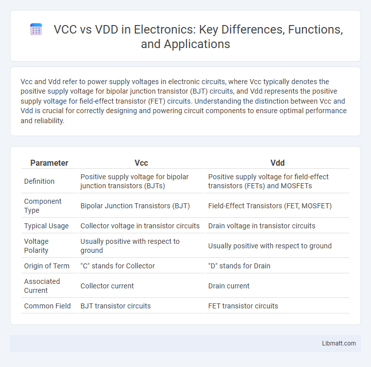
| Parameter | Vcc | Vdd |
|---|---|---|
| Definition | Positive supply voltage for bipolar junction transistors (BJTs) | Positive supply voltage for field-effect transistors (FETs) and MOSFETs |
| Component Type | Bipolar Junction Transistors (BJT) | Field-Effect Transistors (FET, MOSFET) |
| Typical Usage | Collector voltage in transistor circuits | Drain voltage in transistor circuits |
| Voltage Polarity | Usually positive with respect to ground | Usually positive with respect to ground |
| Origin of Term | "C" stands for Collector | "D" stands for Drain |
| Associated Current | Collector current | Drain current |
| Common Field | BJT transistor circuits | FET transistor circuits |
Understanding Vcc and Vdd: Key Differences
Vcc and Vdd are terms used in electronics to denote supply voltages, where Vcc typically refers to the collector supply voltage in bipolar junction transistor (BJT) circuits, while Vdd indicates the drain supply voltage in metal-oxide-semiconductor field-effect transistor (MOSFET) circuits. Vcc is connected to the positive terminal of the power supply in circuits utilizing BJTs, and Vdd is the positive voltage supply in MOSFET-based designs, reflecting different transistor technologies. The key difference lies in their association with transistor types and circuit configurations, making Vcc common in BJT circuits and Vdd prevalent in CMOS and MOSFET circuits.
The Origins of Vcc and Vdd Terminology
Vcc and Vdd terminology originates from the transistor types used in electronic circuits, where Vcc refers to the collector supply voltage in bipolar junction transistors (BJTs) and Vdd pertains to the drain supply voltage in metal-oxide-semiconductor field-effect transistors (MOSFETs). The letters V, C, and D represent voltage, collector, and drain respectively, reflecting the physical terminals in each transistor type. This nomenclature remains standard in circuit design to distinguish power supply connections based on transistor technology.
Common Applications for Vcc and Vdd
Vcc and Vdd are commonly used in electronics to denote power supply voltages, with Vcc referring to the positive voltage supply for bipolar junction transistor (BJT) circuits and Vdd representing the drain voltage in field-effect transistor (FET) circuits. Vcc is typically seen in analog and digital circuits using BJTs, such as amplifiers and logic gates, while Vdd is prevalent in MOSFET-based devices like CMOS integrated circuits and microprocessors. Understanding these applications helps you properly identify power supply pins and optimize circuit design for transistor types.
Role of Vcc in Bipolar Junction Transistors
Vcc represents the positive supply voltage connected to the collector terminal in Bipolar Junction Transistors (BJTs), providing the necessary voltage for proper transistor operation. It establishes the collector-emitter voltage drop, enabling the transistor to amplify current effectively in amplifier circuits. Your circuit's performance depends on the stable Vcc value to maintain consistent transistor switching and amplification.
Role of Vdd in CMOS and MOSFET Circuits
Vdd serves as the primary positive power supply voltage in CMOS and MOSFET circuits, critical for defining the operating point and enabling transistor switching operations. It establishes the necessary voltage difference between the drain and source terminals, influencing the MOSFET's conduction state and overall circuit performance. Maintaining a stable Vdd is essential for reliable logic level representation and power efficiency in integrated circuit designs.
Vcc vs Vdd: Voltage Levels and Standards
Vcc typically refers to the positive supply voltage connected to the collector terminal in bipolar junction transistor (BJT) circuits, commonly standardized around +5V or +12V in many applications. Vdd denotes the positive supply voltage for the drain terminal in field-effect transistor (FET) circuits, often aligning with logic levels such as +3.3V or +5V in CMOS technology. Understanding the voltage levels and standards of Vcc versus Vdd is crucial for designing compatible power supplies and ensuring proper operation of your semiconductor devices.
Circuit Design Considerations: Vcc and Vdd
Vcc and Vdd refer to the supply voltages in circuit design, with Vcc typically representing the positive supply voltage for bipolar junction transistor (BJT) circuits and Vdd denoting the positive voltage supply for MOSFET-based circuits. When designing your circuit, selecting the appropriate voltage level for Vcc or Vdd is crucial to ensure stable operation and optimal transistor switching performance. Proper decoupling and power supply filtering must be implemented to minimize noise and voltage fluctuations that can impact the reliability of both Vcc and Vdd powered circuits.
Labeling Conventions in Schematics: Vcc and Vdd
Vcc and Vdd labeling conventions in schematics denote specific power supply voltages essential for different transistor types; Vcc typically refers to the positive supply voltage for bipolar junction transistors (BJTs), while Vdd indicates the positive supply voltage for field-effect transistors (FETs). These labels help clarify circuit functionality by distinguishing between collector supply voltage (Vcc) and drain supply voltage (Vdd), facilitating accurate design and troubleshooting. Understanding these conventions enables you to interpret schematics correctly and ensures proper component connectivity based on transistor technology.
Typical Mistakes When Using Vcc and Vdd
Typical mistakes when using Vcc and Vdd include confusing the voltage reference points, as Vcc usually denotes the supply voltage for bipolar junction transistors (BJTs) while Vdd refers to the positive supply voltage for MOSFETs. Engineers often mislabel circuits by interchanging these terms, leading to design documentation errors and potential misinterpretation during troubleshooting. Proper identification of the transistor type and corresponding power rails is essential to avoid functional faults and ensure accurate schematic representation.
Choosing the Right Supply: Vcc or Vdd?
Choosing between Vcc and Vdd depends on the transistor technology used in the circuit: Vcc typically refers to the positive supply voltage for bipolar junction transistor (BJT) circuits, while Vdd denotes the positive supply voltage for metal-oxide-semiconductor field-effect transistor (MOSFET) circuits. Understanding the semiconductor type ensures correct voltage application, preventing device damage and optimizing circuit performance. Selecting the appropriate supply voltage label streamlines design documentation and supports clear communication among engineers.
Vcc vs Vdd Infographic