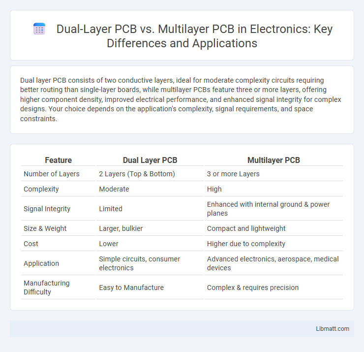
Dual layer PCB consists of two conductive layers, ideal for moderate complexity circuits requiring better routing than single-layer boards, while multilayer PCBs feature three or more layers, offering higher component density, improved electrical performance, and enhanced signal integrity for complex designs. Your choice depends on the application's complexity, signal requirements, and space constraints.
Table of Comparison
| Feature | Dual Layer PCB | Multilayer PCB |
|---|---|---|
| Number of Layers | 2 Layers (Top & Bottom) | 3 or more Layers |
| Complexity | Moderate | High |
| Signal Integrity | Limited | Enhanced with internal ground & power planes |
| Size & Weight | Larger, bulkier | Compact and lightweight |
| Cost | Lower | Higher due to complexity |
| Application | Simple circuits, consumer electronics | Advanced electronics, aerospace, medical devices |
| Manufacturing Difficulty | Easy to Manufacture | Complex & requires precision |
Introduction to Dual Layer and Multilayer PCBs
Dual Layer PCBs consist of two copper layers separated by an insulating substrate, providing increased circuit density and improved electrical performance compared to single-layer boards. Multilayer PCBs incorporate three or more conductive layers stacked together, enabling complex circuit designs, enhanced signal integrity, and higher component density within compact spaces. Both types are essential in modern electronics, with dual-layer boards suitable for moderately complex applications and multilayer PCBs preferred for advanced, high-performance devices.
Structure and Composition of Dual Layer PCBs
Dual Layer PCBs consist of two conductive copper layers separated by an insulating substrate, typically fiberglass-reinforced epoxy resin (FR4). The top and bottom copper layers enable circuit routing on both sides, connected through plated through-holes known as vias. This structure provides enhanced electrical performance and increased component density compared to single-layer PCBs, while maintaining a simpler manufacturing process than multilayer PCBs.
Structure and Composition of Multilayer PCBs
Multilayer PCBs consist of three or more conductive copper layers stacked with insulating prepreg material, providing increased circuit density and enhanced electrical performance compared to dual-layer PCBs, which feature only two copper layers on opposite sides of the substrate. The internal layers of multilayer PCBs are laminated together under high heat and pressure, creating compact, complex circuits suited for advanced electronics. This layered structure allows for improved signal integrity, reduced electromagnetic interference, and greater flexibility in routing intricate circuit paths.
Key Differences Between Dual Layer and Multilayer PCBs
Dual Layer PCBs consist of two conductive copper layers, allowing for moderate circuit complexity and improved signal routing compared to single-layer boards. Multilayer PCBs have three or more layers stacked together, providing higher density, enhanced electrical performance, and better electromagnetic interference (EMI) management. Your choice between dual layer and multilayer PCBs depends on the complexity, size, and performance requirements of your electronic design.
Electrical Performance Comparison
Dual layer PCBs offer improved electrical performance over single-layer boards by providing two conductive layers for signal routing and power distribution, reducing signal interference and crosstalk. Multilayer PCBs enhance electrical performance further by incorporating multiple signal and ground planes, which enable better impedance control, reduced electromagnetic interference (EMI), and higher signal integrity, essential for high-speed and complex circuits. The increased layer count in multilayer boards supports denser component placement and optimized power distribution networks, resulting in superior noise reduction and improved overall electrical reliability.
Manufacturing Process Differences
Dual layer PCB manufacturing involves etching conductive layers on both sides of a single substrate, requiring precise alignment for drilling vias and applying solder masks. Multilayer PCB fabrication incorporates stacking alternating layers of dielectric material and conductive copper sheets, bonded under heat and pressure to achieve complex circuit designs with multiple internal layers. The multilayer process demands advanced lamination and via formation techniques such as blind and buried vias to ensure signal integrity and mechanical stability.
Cost Analysis: Dual Layer vs Multilayer PCBs
Dual layer PCBs typically offer a lower initial cost compared to multilayer PCBs due to simpler manufacturing processes and fewer material requirements. Multilayer PCBs, though more expensive upfront, can reduce assembly costs by integrating more complex circuits into a compact design, potentially lowering overall system expenses. Your choice should balance budget constraints with performance needs, as multilayer PCBs provide better signal integrity and design flexibility at a higher cost.
Applications and Use Cases
Dual layer PCBs are commonly used in applications requiring moderate circuit density, such as consumer electronics, automotive control systems, and power supplies, where cost-efficiency and easier manufacturing are priorities. Multilayer PCBs support complex, high-density designs with multiple signal layers and ground planes, making them ideal for advanced computing devices, aerospace equipment, and telecommunications infrastructure. Your choice depends on the complexity and performance demands of the application, with multilayer PCBs suited for high-speed, high-frequency, and miniaturized circuit requirements.
Advantages and Disadvantages
Dual layer PCBs offer simpler design and lower cost compared to multilayer PCBs, making them ideal for basic electronic circuits with limited complexity. Multilayer PCBs provide higher circuit density, improved signal integrity, and better electrical performance, suitable for advanced applications requiring compact design and multiple signal layers. Your choice depends on balancing the need for complexity, space constraints, and budget considerations.
How to Choose Between Dual Layer and Multilayer PCBs
Choosing between dual layer and multilayer PCBs depends on the complexity of your electronic design and space constraints. Dual layer PCBs offer simpler routing and lower manufacturing costs, ideal for moderate circuit density and basic applications. Multilayer PCBs provide higher component density and enhanced electrical performance, making them suitable for advanced devices requiring compact size and superior signal integrity.
Dual Layer PCB vs Multilayer PCB Infographic