SOIC (Small Outline Integrated Circuit) offers a more compact, surface-mount solution compared to the through-hole DIP (Dual In-line Package), which is larger and easier to prototype on breadboards. Your choice depends on the available PCB space and manufacturing capabilities, with SOIC preferred for high-density designs and DIP for simpler, manual assembly.
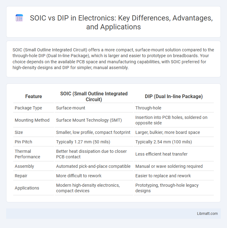
Table of Comparison
| Feature | SOIC (Small Outline Integrated Circuit) | DIP (Dual In-line Package) |
|---|---|---|
| Package Type | Surface-mount | Through-hole |
| Mounting Method | Surface Mount Technology (SMT) | Insertion into PCB holes, soldered on opposite side |
| Size | Smaller, low profile, compact footprint | Larger, bulkier, more board space |
| Pin Pitch | Typically 1.27 mm (50 mils) | Typically 2.54 mm (100 mils) |
| Thermal Performance | Better heat dissipation due to closer PCB contact | Less efficient heat transfer |
| Assembly | Automated pick-and-place compatible | Manual or wave soldering required |
| Repair | More difficult to rework | Easier to replace and rework |
| Applications | Modern high-density electronics, compact devices | Prototyping, through-hole legacy designs |
Introduction to SOIC and DIP Packages
SOIC (Small Outline Integrated Circuit) and DIP (Dual In-line Package) are two common types of IC packaging used in electronics. SOIC packages feature a compact, surface-mount design with gull-wing leads that facilitate automated PCB assembly, while DIP packages have through-hole pins arranged in two parallel rows, making them suitable for prototyping and manual insertion. Your choice between SOIC and DIP depends on factors such as board space, assembly method, and application requirements.
Historical Overview of IC Packaging
The historical development of IC packaging highlights SOIC (Small Outline Integrated Circuit) and DIP (Dual In-line Package) as milestone technologies in semiconductor advancements. DIP technology, introduced in the 1960s, became foundational for through-hole mounting on printed circuit boards (PCBs) due to its ease of handling and reliable connections. SOIC packages emerged in the 1980s as a surface-mount alternative, offering reduced footprint and improved electrical performance to support the miniaturization trends in electronic device design.
Physical Differences Between SOIC and DIP
SOIC (Small Outline Integrated Circuit) packages are surface-mount devices characterized by their flat, rectangular shape and shorter lead lengths, allowing for compact PCB layouts with reduced profile height compared to DIP (Dual Inline Package). DIP components feature through-hole mounting with two parallel rows of pins extending perpendicularly from the package, making them bulkier and more suitable for prototyping and manual assembly. Your choice between SOIC and DIP influences soldering technique, board space efficiency, and overall device miniaturization.
Electrical Performance: SOIC vs DIP
SOIC (Small Outline Integrated Circuit) packages offer lower parasitic inductance and capacitance compared to DIP (Dual In-Line Package) designs, resulting in improved electrical performance at higher frequencies. The reduced lead length in SOIC minimizes signal distortion and crosstalk, which is critical for your high-speed or RF circuit applications. DIP packages, while easier for prototyping, typically exhibit higher noise susceptibility due to their larger lead inductance and greater parasitic effects.
Assembly and Soldering Considerations
SOIC (Small Outline Integrated Circuit) packages feature surface-mount technology, making their assembly and soldering processes suitable for automated pick-and-place machines and reflow soldering, which ensures precise placement and minimal solder bridging. DIP (Dual In-line Package) components require through-hole mounting, often involving manual insertion followed by wave soldering or selective soldering, which might be more time-consuming and less compatible with high-volume automated assembly lines. Your choice between SOIC and DIP influences manufacturing efficiency and solder joint reliability based on the available assembly equipment and process requirements.
Space and Density Comparison
SOIC packages offer a significantly smaller footprint and higher pin density compared to DIP counterparts, making them ideal for space-constrained PCB designs. The surface-mount nature of SOICs eliminates the need for through-hole mounting, enabling closer component placement and more efficient board layouts. DIP packages, while easier to handle and prototype with, consume more board space and have lower pin density, limiting their use in compact, high-density applications.
Cost and Availability Analysis
SOIC (Small Outline Integrated Circuit) packages typically offer lower production costs and greater availability due to their compact size and widespread use in modern electronics manufacturing. DIP (Dual Inline Package) components may have higher costs and limited availability as they are generally considered legacy parts, mainly used in prototyping or through-hole designs. Your choice largely depends on balancing budget constraints with the need for component sourcing, where SOIC often provides more cost-effective and readily accessible options.
Application Suitability: SOIC vs DIP
SOIC (Small Outline Integrated Circuit) packages are ideal for high-density, surface-mount applications on printed circuit boards where space-saving and automated assembly are critical. DIP (Dual In-line Package) components suit through-hole prototyping and repairs, offering ease of manual handling and insertion into breadboards or sockets. Your choice between SOIC and DIP should align with manufacturing needs, with SOIC favored for compact, mass-produced electronics and DIP preferred for simple, flexible testing or educational projects.
Pros and Cons of Each Package
SOIC (Small Outline Integrated Circuit) packages offer a compact form factor with reduced lead length, which enhances electrical performance by minimizing parasitic inductance and capacitance, making them ideal for high-speed applications. However, their smaller size can complicate manual soldering and repair compared to DIP (Dual Inline Package) components, which feature larger, more spaced leads that simplify prototyping and handling. DIP packages are advantageous for ease of insertion into breadboards and sockets but consume more PCB space and have slower signal transmission due to longer lead lengths.
Choosing the Right Package for Your Project
Selecting between SOIC (Small Outline Integrated Circuit) and DIP (Dual Inline Package) depends on project requirements such as board space, ease of handling, and soldering method. SOIC offers a compact, surface-mount solution ideal for high-density PCB layouts, while DIP provides a larger, through-hole design favored for prototyping and manual assembly. Evaluating factors like available PCB real estate, automated manufacturing capabilities, and repair convenience ensures the appropriate package choice aligned with project goals.
SOIC vs DIP Infographic