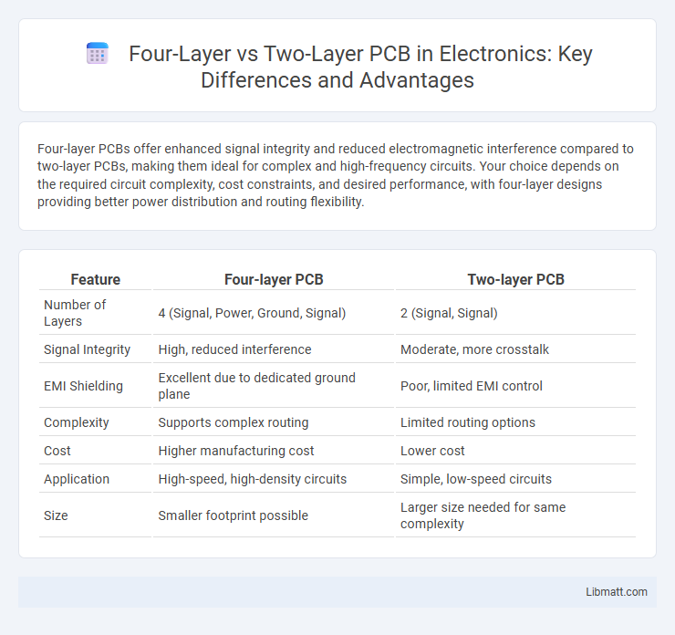
Four-layer PCBs offer enhanced signal integrity and reduced electromagnetic interference compared to two-layer PCBs, making them ideal for complex and high-frequency circuits. Your choice depends on the required circuit complexity, cost constraints, and desired performance, with four-layer designs providing better power distribution and routing flexibility.
Table of Comparison
| Feature | Four-layer PCB | Two-layer PCB |
|---|---|---|
| Number of Layers | 4 (Signal, Power, Ground, Signal) | 2 (Signal, Signal) |
| Signal Integrity | High, reduced interference | Moderate, more crosstalk |
| EMI Shielding | Excellent due to dedicated ground plane | Poor, limited EMI control |
| Complexity | Supports complex routing | Limited routing options |
| Cost | Higher manufacturing cost | Lower cost |
| Application | High-speed, high-density circuits | Simple, low-speed circuits |
| Size | Smaller footprint possible | Larger size needed for same complexity |
Introduction to PCB Layer Configurations
Four-layer PCB configurations consist of two signal layers sandwiched between two ground and power planes, providing enhanced electromagnetic interference (EMI) shielding and improved signal integrity compared to two-layer PCBs, which only have one signal layer on each side. Four-layer boards support more complex circuit designs by allowing better power distribution and reducing crosstalk, making them ideal for high-speed and high-density applications. Your choice depends on factors like circuit complexity, cost constraints, and performance requirements.
Understanding Two-Layer PCB Design
Two-layer PCB design uses two conductive copper layers separated by a dielectric, allowing for improved circuit density and better signal routing compared to single-layer PCBs. This design supports more complex electronic components and provides enhanced electrical performance through reduced electromagnetic interference and signal crosstalk. Two-layer PCBs are cost-effective solutions ideal for moderate-complexity applications such as consumer electronics, automotive sensors, and communication devices.
Overview of Four-Layer PCB Architecture
Four-layer PCB architecture consists of two signal layers and two internal layers dedicated to power and ground planes, enhancing electrical performance and noise reduction. This structure improves signal integrity and electromagnetic interference (EMI) shielding compared to two-layer PCBs, making it ideal for complex and high-speed circuits. Your designs benefit from better thermal management and routing flexibility due to the additional layers in four-layer PCBs.
Key Differences Between Two-Layer and Four-Layer PCBs
Two-layer PCBs consist of two conductive layers separated by an insulating substrate, providing basic circuit complexity suitable for simpler electronic devices, while four-layer PCBs incorporate two additional internal layers dedicated to power and ground planes, enhancing signal integrity and reducing electromagnetic interference. Four-layer PCBs support more advanced routing options, increased circuit density, and improved thermal management compared to two-layer PCBs. Your choice depends on the complexity, performance requirements, and budget constraints of your electronic design.
Signal Integrity and Electromagnetic Interference
Four-layer PCBs offer superior signal integrity compared to two-layer PCBs due to dedicated ground and power planes that provide consistent impedance control and reduce signal crosstalk. The additional layers allow for better electromagnetic interference (EMI) shielding, minimizing noise and enhancing overall PCB performance in high-frequency applications. Two-layer PCBs, while cost-effective, lack these isolation and grounding benefits, making them more susceptible to signal degradation and EMI issues.
Thermal Management in PCB Layers
Four-layer PCBs offer superior thermal management compared to two-layer PCBs due to the additional inner layers that facilitate better heat dissipation and distribution. These inner copper planes act as heat sinks, reducing hotspots and enhancing the reliability of high-power or high-frequency circuits. Optimizing your design with four-layer PCBs ensures efficient heat transfer, crucial for maintaining performance and longevity in complex electronic devices.
Cost Implications: Two-Layer vs Four-Layer PCBs
Two-layer PCBs generally offer lower production costs due to simpler manufacturing processes and reduced material usage, making them ideal for budget-sensitive projects. Four-layer PCBs involve higher expenses driven by added layers, increased complexity, and longer fabrication times, but provide enhanced signal integrity and design flexibility. Your choice between two-layer and four-layer PCBs should weigh initial cost savings against potential performance benefits and long-term reliability requirements.
Performance and Reliability Considerations
Four-layer PCBs offer enhanced signal integrity and reduced electromagnetic interference due to dedicated power and ground planes, improving overall performance compared to two-layer PCBs. The additional layers provide better thermal management and mechanical strength, which significantly increases reliability in high-frequency and complex circuit applications. Two-layer PCBs may suffice for simpler designs but often face limitations in noise reduction and durability under demanding conditions.
Application Suitability: Which Layer Count Fits Your Project?
Two-layer PCBs are suitable for simple, low-density circuits commonly used in consumer electronics and basic embedded systems, offering cost efficiency and easier manufacturing. Four-layer PCBs provide enhanced signal integrity, better electromagnetic interference (EMI) shielding, and improved power distribution, making them ideal for complex applications such as high-speed communication devices and multi-functional industrial equipment. Choosing between two-layer and four-layer PCBs depends on the design complexity, signal requirements, and budget constraints of the specific project.
Conclusion: Choosing the Right PCB Layer Structure
Four-layer PCBs offer enhanced signal integrity, better electromagnetic interference (EMI) control, and increased routing density compared to two-layer PCBs, making them ideal for complex or high-frequency designs. Two-layer PCBs remain cost-effective and suitable for simpler circuits with lower component counts and less demanding performance requirements. Your choice should align with application complexity, budget constraints, and performance needs to ensure optimal functionality and manufacturing efficiency.
Four-layer vs Two-layer PCB Infographic