FET (Field Effect Transistor) and JFET (Junction Field Effect Transistor) differ primarily in their gate control mechanisms, where JFET uses a reverse-biased p-n junction to control current flow, offering high input impedance and low noise for amplification tasks. Your choice depends on the specific circuit requirements, as FETs include various types like MOSFETs with insulated gates, providing greater voltage control and switching speed compared to JFETs.
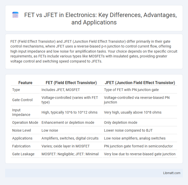
Table of Comparison
| Feature | FET (Field Effect Transistor) | JFET (Junction Field Effect Transistor) |
|---|---|---|
| Type | Includes JFET, MOSFET | Type of FET with PN junction gate |
| Gate Control | Voltage-controlled (varies with FET type) | Voltage-controlled via reverse-biased PN junction |
| Input Impedance | High, typically 10^6 to 10^12 ohms | Very high, usually above 10^8 ohms |
| Operation Mode | Enhancement or depletion mode | Only depletion mode |
| Noise Level | Low noise | Lower noise compared to BJT |
| Applications | Amplifiers, switches, digital circuits | Low noise amplifiers, analog switches |
| Fabrication | Varies; oxide layer in MOSFET | PN junction gate formed in semiconductor |
| Gate Leakage | MOSFET: Negligible; JFET: Minimal | Very low due to reverse-biased gate junction |
Introduction to FET and JFET
Field Effect Transistors (FETs) are semiconductor devices that control current flow using an electric field, offering high input impedance and low power consumption. Junction Field Effect Transistors (JFETs), a subtype of FETs, utilize a reverse-biased p-n junction to regulate current through the channel, typically featuring n-channel or p-channel configurations. Both FET and JFET devices are fundamental in amplifiers and switching applications, valued for their voltage-controlled operation and minimal input current.
Basic Structure of FET
The basic structure of a Field-Effect Transistor (FET) consists of a semiconductor channel, typically made of silicon, with three terminals: the source, drain, and gate. The gate controls the current flow through the channel by applying a voltage that modulates the conductivity without direct current flow into the gate terminal. Unlike Bipolar Junction Transistors, FETs operate with voltage-controlled input impedance, making them ideal for high-impedance and low-noise applications.
Understanding JFET Architecture
JFET (Junction Field-Effect Transistor) architecture features a channel of semiconductor material with p-n junctions on both sides, controlling current flow through voltage applied to the gate terminal. The gate forms a depletion region that modulates conductivity, allowing the JFET to operate as a voltage-controlled resistor, offering high input impedance and low noise characteristics. Unlike FETs with insulated gates, the JFET's gate junction prevents current flow, making it suitable for analog applications requiring consistent gate control.
Key Differences Between FET and JFET
FET (Field Effect Transistor) is a broad category of transistors controlled by an electric field, while JFET (Junction Field Effect Transistor) is a specific type of FET using a reverse-biased p-n junction to control current flow. The JFET operates only in depletion mode and offers high input impedance and low noise, making it ideal for amplifying weak signals. Understanding these key differences helps you select the appropriate transistor for your electronic circuit designs based on control mechanism and operational characteristics.
Working Principle of FET
The working principle of a Field-Effect Transistor (FET) relies on controlling the current flow through a semiconductor channel by applying voltage to the gate terminal, which modulates the channel's conductivity without any direct current flow into the gate. Unlike Bipolar Junction Transistors (BJTs), FETs use an electric field to control the shape and width of the conductive channel, making them voltage-driven devices with high input impedance. Your circuit efficiency benefits from FET's ability to act as a precise electronic switch or amplifier with minimal power consumption and reduced noise levels.
Operation of JFET
JFET operates by controlling current flow through a semiconductor channel using a reverse-biased p-n junction, which forms a depletion region that modulates conductivity. When voltage is applied to the gate terminal, it widens the depletion region, restricting current flow between the source and drain terminals. Your circuits benefit from JFET's high input impedance and low noise operation, making it ideal for sensitive analog signal applications.
Advantages of FET Over JFET
Field-Effect Transistors (FETs) offer greater versatility and higher input impedance compared to Junction Field-Effect Transistors (JFETs), enhancing their performance in low-noise and high-frequency applications. Unlike JFETs, Metal-Oxide-Semiconductor FETs (MOSFETs), a type of FET, provide better scalability and faster switching speeds, making them ideal for digital circuits and power management. The ability to operate with enhancement mode also allows FETs a wider range of applications than the primarily depletion-mode JFETs.
Limitations of JFET Technology
JFET technology faces limitations including lower input voltage range and inability to handle high-frequency applications compared to FETs. Its restricted gate voltage swing limits the voltage amplification capability, making it less suitable for modern high-speed circuits. You may find FETs more advantageous for broader frequency responses and higher input impedance in advanced electronic designs.
Applications of FET and JFET
FETs (Field Effect Transistors) are widely used in amplifiers, switches, and voltage-controlled resistors due to their high input impedance and low noise, making them ideal for audio and RF circuits. JFETs (Junction Field Effect Transistors) excel in low-noise applications such as sensitive preamplifiers and analog signal processing, benefiting from their simple construction and stable operation. You can select FETs for general-purpose amplification and switching tasks, while JFETs are preferred in precision analog circuits requiring minimal signal distortion.
Future Trends in FET and JFET Development
Advancements in FET technology focus on wide-bandgap materials like GaN and SiC, enabling higher power efficiency and faster switching speeds in applications such as 5G and electric vehicles. JFET research aims to enhance low-noise and high-frequency performance by optimizing channel doping and device miniaturization for sensors and RF circuits. Integration of FETs and JFETs with silicon photonics and flexible electronics represents a significant trend driving next-generation communication and wearable devices.
FET vs JFET Infographic