Conductive vias provide electrical connections through multiple layers of a printed circuit board (PCB), facilitating signal or power transfer from one side of the board to the other. Blind vias connect outer layers to one or more inner layers without passing through the entire PCB, optimizing your board layout by saving space and improving signal integrity.
Table of Comparison
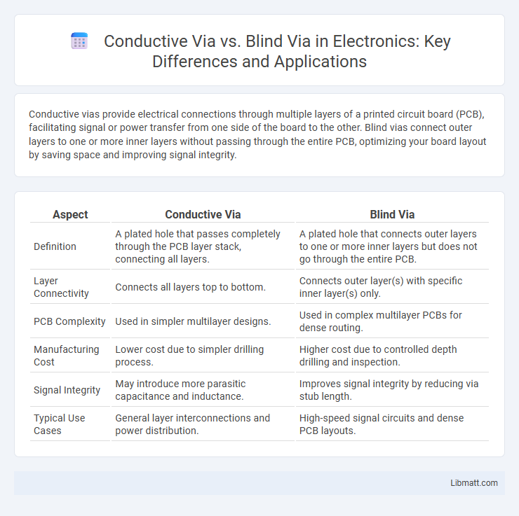
| Aspect | Conductive Via | Blind Via |
|---|---|---|
| Definition | A plated hole that passes completely through the PCB layer stack, connecting all layers. | A plated hole that connects outer layers to one or more inner layers but does not go through the entire PCB. |
| Layer Connectivity | Connects all layers top to bottom. | Connects outer layer(s) with specific inner layer(s) only. |
| PCB Complexity | Used in simpler multilayer designs. | Used in complex multilayer PCBs for dense routing. |
| Manufacturing Cost | Lower cost due to simpler drilling process. | Higher cost due to controlled depth drilling and inspection. |
| Signal Integrity | May introduce more parasitic capacitance and inductance. | Improves signal integrity by reducing via stub length. |
| Typical Use Cases | General layer interconnections and power distribution. | High-speed signal circuits and dense PCB layouts. |
Introduction to Conductive Via and Blind Via
Conductive vias are crucial electrical connections in multilayer printed circuit boards (PCBs) that pass through all layers, providing continuous pathways for signals and power. Blind vias, in contrast, connect only outer layers to one or more inner layers without penetrating the entire board, optimizing space and improving circuit density. Your PCB design benefits from understanding these via types to enhance performance, reduce manufacturing complexity, and maximize component placement efficiency.
Definitions: What Are Conductive Vias and Blind Vias?
Conductive vias are plated through-holes that establish electrical connections between all layers in a multi-layer printed circuit board (PCB). Blind vias connect only the outer layer to one or more inner layers without passing completely through the PCB. Understanding the difference between these via types helps optimize your PCB design for signal integrity and manufacturing cost.
Key Differences Between Conductive Vias and Blind Vias
Conductive vias are through-hole connections that create electrical pathways by passing completely through the PCB, allowing signals to travel from one layer to another. Blind vias, on the other hand, connect only an outer layer to one or more inner layers without piercing the entire board, optimizing space in high-density PCB designs. The key differences lie in their structural depth, electrical performance, and application flexibility, where conductive vias offer straightforward connectivity while blind vias enable compact layouts and improved signal integrity in multilayer circuits.
Applications of Conductive Vias in PCB Design
Conductive vias play a crucial role in PCB design by enabling electrical connections between different layers, essential for multilayer circuit boards in applications like smartphones, computers, and automotive electronics. These vias support high-density interconnects and efficient signal transmission, improving overall board performance and reliability. Your PCB design benefits from conductive vias by optimizing space and enhancing thermal management where through-hole and buried vias can't be effectively used.
Applications of Blind Vias in Advanced Circuits
Blind vias are widely used in advanced circuits to connect outer layers with inner layers without penetrating the entire PCB, thereby saving space and enabling higher component density. They are essential in high-frequency and high-speed designs, such as smartphones and compact IoT devices, where minimizing signal loss and crosstalk is critical. Their application improves signal integrity and supports complex multilayer stack-ups in modern electronics manufacturing.
Manufacturing Processes for Conductive and Blind Vias
Manufacturing processes for conductive vias involve drilling holes completely through the printed circuit board (PCB) followed by plating with copper to establish electrical connectivity between all layers. Blind vias are created by drilling holes that penetrate only from the surface to an inner layer, requiring precise depth control and advanced laser or mechanical drilling techniques to prevent damage to inner layers. Both processes necessitate meticulous plating to ensure reliable conductivity and structural integrity within high-density interconnect (HDI) PCBs.
Electrical Performance: Conductive Via vs Blind Via
Conductive vias provide consistent electrical performance by enabling full vertical signal conduction through the entire PCB layer stack, ensuring minimal resistance and inductance. Blind vias, connecting only outer layers to specific inner layers, reduce signal path length and parasitic capacitance, enhancing high-frequency performance in multilayer designs. Your choice between conductive and blind vias impacts signal integrity, impedance control, and overall circuit efficiency, particularly in high-speed or RF applications.
Cost Implications: Comparing Conductive and Blind Vias
Conductive vias, typically through-hole, involve drilling and plating through the entire PCB thickness, resulting in higher material and manufacturing costs compared to blind vias, which connect outer layers to one or more inner layers without penetrating the entire board. Blind vias reduce layer count and save board space, leading to more compact designs but require advanced fabrication techniques that can increase per-unit cost for complex PCBs. The overall cost implications depend on PCB complexity, layer count, and volume, with conductive vias being more economical for simpler, multi-layer boards, while blind vias offer cost benefits in high-density, high-layer-count applications.
Design Challenges and Considerations
Conductive vias require careful management of plating thickness and hole alignment to ensure reliable electrical connectivity through multiple PCB layers, posing challenges in maintaining uniform conductivity and preventing defects. Blind vias, connecting outer layers to inner layers without penetrating the entire board, demand precise drilling and advanced laser technology to control depth and aspect ratio, increasing manufacturing complexity and cost. Both via types necessitate rigorous design considerations for thermal expansion, signal integrity, and layer stack-up compatibility to optimize performance and reliability in high-density circuit designs.
Choosing the Right Via Type for Your PCB Project
Choosing the right via type for your PCB project depends on factors like design complexity, layer count, and cost constraints. Conductive vias, which pass through all layers, offer reliable electrical connections but consume more space and increase fabrication costs. Blind vias connect outer layers to one or more inner layers without going through the entire board, saving space and improving signal integrity in high-density PCB designs.
Conductive via vs Blind via Infographic