JTAG and SWD are both debugging interfaces used to program and debug microcontrollers, with JTAG offering a 4 or 5-pin interface supporting complex and multi-core devices, while SWD uses a simpler 2-pin interface optimized for ARM Cortex-M processors. Your choice depends on the target device requirements, as SWD provides faster communication with fewer pins, but JTAG supports a wider range of devices and advanced features.
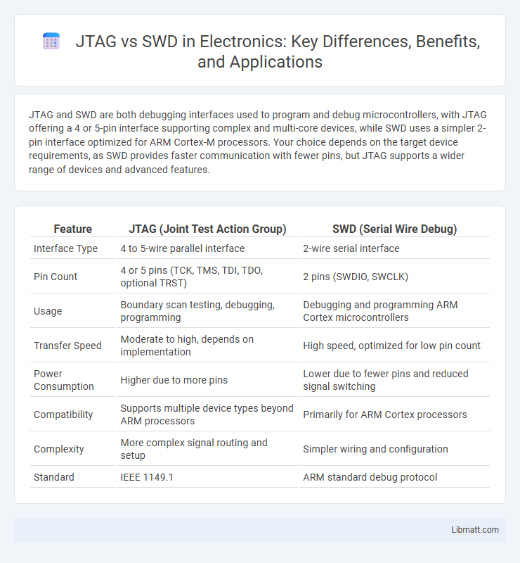
Table of Comparison
| Feature | JTAG (Joint Test Action Group) | SWD (Serial Wire Debug) |
|---|---|---|
| Interface Type | 4 to 5-wire parallel interface | 2-wire serial interface |
| Pin Count | 4 or 5 pins (TCK, TMS, TDI, TDO, optional TRST) | 2 pins (SWDIO, SWCLK) |
| Usage | Boundary scan testing, debugging, programming | Debugging and programming ARM Cortex microcontrollers |
| Transfer Speed | Moderate to high, depends on implementation | High speed, optimized for low pin count |
| Power Consumption | Higher due to more pins | Lower due to fewer pins and reduced signal switching |
| Compatibility | Supports multiple device types beyond ARM processors | Primarily for ARM Cortex processors |
| Complexity | More complex signal routing and setup | Simpler wiring and configuration |
| Standard | IEEE 1149.1 | ARM standard debug protocol |
Introduction to JTAG and SWD
JTAG (Joint Test Action Group) is a widely used standard for verifying designs and testing printed circuit boards through a 4 to 5-wire interface enabling boundary-scan testing and programming. SWD (Serial Wire Debug) is a two-wire protocol developed by ARM designed specifically for efficient debugging and programming of ARM Cortex microcontrollers with reduced pin requirements. Both JTAG and SWD facilitate device debugging and programming but differ in interface complexity, pin usage, and application scope.
Overview of Debugging Protocols
JTAG (Joint Test Action Group) and SWD (Serial Wire Debug) are essential debugging protocols for embedded systems, facilitating communication between a debugger and a microcontroller. JTAG is a standard 4- or 5-wire interface known for supporting boundary-scan testing and complex multi-device debugging, whereas SWD uses a simpler 2-wire interface optimized for ARM Cortex processors, offering efficient and faster debugging. Your choice between JTAG and SWD depends on device compatibility, pin constraints, and debugging complexity requirements.
JTAG: Features and Functionality
JTAG (Joint Test Action Group) is a standard interface used for verifying designs and testing printed circuit boards after manufacture. It supports boundary-scan testing, device programming, and debugging with multiple devices connected in a daisy-chain configuration, facilitating comprehensive system-level diagnostics. JTAG features include multiple test access ports, support for complex device hierarchies, and standardized signaling protocols that enable precise control over silicon chips during development and troubleshooting.
SWD: Features and Functionality
SWD (Serial Wire Debug) features a a two-pin interface for efficient communication between your debugger and microcontroller, reducing pin count compared to traditional JTAG. It supports high-speed data transfer, real-time debugging, and memory access, making it ideal for embedded systems with limited IO resources. SWD functionality includes breakpoint setting, watchpoints, and single-step execution, providing precise control over program execution during development.
Key Differences Between JTAG and SWD
JTAG (Joint Test Action Group) and SWD (Serial Wire Debug) are both debugging protocols used for embedded systems, but they differ primarily in interface complexity and pin count. JTAG uses a 4 or 5-pin interface supporting multiple devices in a chain, providing broad compatibility and advanced test functions, while SWD employs a simpler 2-pin configuration, making it ideal for resource-constrained systems. Your choice between JTAG and SWD will depend on the specific debugging needs, with SWD favored for ARM Cortex-M microcontrollers due to its streamlined hardware requirements.
Hardware Requirements for JTAG and SWD
JTAG hardware requires a minimum of four to five dedicated pins including TCK, TMS, TDI, TDO, and optionally TRST for test reset, necessitating more complex and larger connectors. SWD simplifies hardware requirements by using only two bidirectional pins, SWDIO and SWCLK, reducing PCB complexity and minimizing pin count on microcontrollers. This makes SWD especially suited for resource-constrained embedded systems and compact debugging interfaces.
Performance Comparison: Speed and Efficiency
JTAG and SWD differ significantly in performance, with SWD offering faster data transfer rates and more efficient pin usage due to its two-wire interface compared to JTAG's multi-wire setup. This streamlined protocol allows SWD to achieve quicker debugging cycles and lower latency, enhancing Your ability to perform rapid firmware updates and real-time system analysis. JTAG's broader compatibility supports complex debugging but at the cost of slower speed and increased hardware complexity, making SWD the preferred choice for speed-critical embedded development.
Industry Adoption and Use Cases
JTAG remains widely adopted in industries requiring comprehensive boundary-scan testing and debugging, particularly in aerospace, automotive, and complex multi-core processor environments. SWD is predominant in embedded systems and microcontroller development, offering a streamlined, lower-pin alternative ideal for ARM Cortex-M devices frequently used in IoT and consumer electronics. Your choice between JTAG and SWD should consider device compatibility, pin availability, and specific debugging requirements aligned with your project's industry standards.
Security Considerations
JTAG and SWD protocols differ significantly in security considerations, as JTAG's broader pin interface poses a higher risk of unauthorized access compared to the more streamlined SWD. Secure implementations often limit JTAG functionality or disable it entirely after programming to prevent extraction of sensitive data or firmware. For Your device's protection, adopting SWD with proper authentication and access control mechanisms reduces vulnerability to hardware tampering and reverse engineering attempts.
Choosing the Right Protocol for Your Project
JTAG and SWD are both popular debugging interfaces, with JTAG offering multi-pin connectivity suited for complex devices, while SWD provides a two-pin interface optimized for ARM Cortex microcontrollers. Choose JTAG when needing advanced debugging features, boundary scan testing, or compatibility with a wide range of devices. Opt for SWD in projects requiring minimal pin usage, faster programming, and efficient debugging on ARM-based embedded systems.
JTAG vs SWD Infographic