Edge coupling involves placing transmission lines side-by-side, enabling electromagnetic fields to interact along their edges, which offers tighter coupling and higher coupling coefficients. Broadside coupling aligns transmission lines one above the other, increasing the overlap area and providing better isolation and reduced radiation, enhancing your circuit's performance in high-frequency applications.
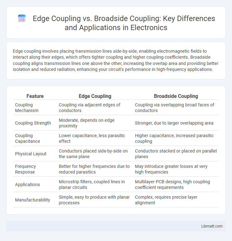
Table of Comparison
| Feature | Edge Coupling | Broadside Coupling |
|---|---|---|
| Coupling Mechanism | Coupling via adjacent edges of conductors | Coupling via overlapping broad faces of conductors |
| Coupling Strength | Moderate, depends on edge proximity | Stronger, due to larger overlapping area |
| Coupling Capacitance | Lower capacitance, less parasitic effect | Higher capacitance, increased parasitic coupling |
| Physical Layout | Conductors placed side-by-side on the same plane | Conductors stacked or placed on parallel planes |
| Frequency Response | Better for higher frequencies due to reduced parasitics | May introduce greater losses at very high frequencies |
| Applications | Microstrip filters, coupled lines in planar circuits | Multilayer PCB designs, high coupling coefficient requirements |
| Manufacturability | Simple, easy to produce with planar processes | Complex, requires precise layer alignment |
Introduction to Edge and Broadside Coupling
Edge coupling occurs when two transmission lines are placed adjacent to each other along their edges, facilitating capacitive and inductive interaction that affects signal propagation and crosstalk. Broadside coupling involves one transmission line positioned directly above another, separated by a dielectric layer, increasing coupling efficiency due to larger overlapping surfaces. This method often results in stronger electromagnetic coupling and improved control over impedance characteristics in high-frequency circuit designs.
Fundamentals of PCB Trace Coupling
Edge coupling and broadside coupling are fundamental PCB trace coupling methods that influence signal integrity and electromagnetic interference. Edge coupling places two microstrip traces side-by-side on the same layer, optimizing differential impedance through the narrow spacing of edges, ideal for high-frequency signal transmission. Broadside coupling stacks traces vertically on adjacent layers, increasing capacitive coupling and allowing controlled impedance with reduced crosstalk in multilayer PCB designs.
What is Edge Coupling?
Edge coupling is a technique in microwave engineering where two transmission lines run parallel with their edges closely spaced to achieve capacitive and inductive coupling. This method enables controlled signal interaction primarily through the fringing fields at the edges, making it suitable for coupling in microstrip lines and stripline configurations. Edge coupling provides a compact design approach with predictable coupling coefficients essential for filters and directional couplers in RF circuits.
Understanding Broadside Coupling
Broadside coupling occurs when two conductive elements are placed parallel and directly facing each other on different layers of a PCB, creating a stronger capacitive link compared to edge coupling. This configuration enhances signal integrity by reducing electromagnetic interference and crosstalk, making it ideal for high-frequency applications. Understanding broadside coupling helps optimize your PCB design for improved performance and reduced signal loss.
Key Differences Between Edge and Broadside Coupling
Edge coupling features conductors placed side-by-side on the same plane, resulting in stronger electrostatic fields and typically higher coupling capacitance, while broadside coupling aligns conductors on parallel planes stacked vertically, offering enhanced magnetic coupling and lower crosstalk. Your choice between edge and broadside coupling affects signal integrity, with edge coupling often preferred for narrow, high-frequency traces and broadside coupling providing better isolation and bandwidth in multi-layer PCB designs. Key differences include layout complexity, coupling strength, and electromagnetic interference characteristics, which directly influence your circuit's performance and design constraints.
Signal Integrity in Edge vs Broadside Coupling
Edge coupling offers improved signal integrity in high-frequency PCB designs by minimizing crosstalk through tighter control of the electric field between adjacent traces, resulting in lower insertion loss and better impedance matching. Broadside coupling, with its parallel conductor layers separated by a dielectric, provides enhanced coupling capacitance, which can reduce signal leakage but may introduce greater parasitic inductance and increased susceptibility to noise. Optimizing signal integrity depends on selecting edge coupling for precise impedance control in differential pairs and broadside coupling where increased capacitive coupling aids in noise reduction over longer transmission lines.
Crosstalk Considerations in PCB Design
Edge coupling and broadside coupling significantly influence crosstalk in PCB design, with edge coupling generally causing stronger near-end crosstalk due to tighter field interaction between adjacent traces. Broadside coupling offers better control over crosstalk by leveraging greater trace separation and directional field alignment, which reduces signal interference in high-speed layouts. Understanding these differences helps optimize your PCB layout for minimal crosstalk, improving signal integrity and overall circuit performance.
Design Guidelines for Edge Coupling
Design guidelines for edge coupling emphasize maintaining precise control over the gap between the adjacent conductor edges to ensure efficient electromagnetic energy transfer in planar transmission lines. The width of the coupled edges and the dielectric constant of the substrate directly influence coupling strength and signal integrity, necessitating careful material selection and dimensional accuracy. Proper spacing and conductor width optimization minimize crosstalk and insertion loss, enhancing performance in high-frequency RF and microwave circuit designs.
Design Guidelines for Broadside Coupling
Broadside coupling in microwave circuits involves placing transmission lines on different layers with overlapping widths, which enhances coupling strength and reduces crosstalk compared to edge coupling. Design guidelines recommend maintaining precise layer alignment, controlling the dielectric thickness to optimize coupling capacitance, and selecting appropriate trace widths and spacing to achieve desired coupling coefficients. Your PCB layout should ensure minimized fabrication tolerances and consider utilizing broadside coupling for tighter coupling requirements in compact RF designs.
Choosing the Best Coupling Method for Your Application
Edge coupling and broadside coupling both offer distinct advantages depending on your application's frequency range and layout constraints. Edge coupling provides tighter coupling and better isolation at higher frequencies due to the proximity of conductor edges, making it ideal for compact microwave circuits. Broadside coupling, with larger overlapping conductor surfaces, yields higher coupling coefficients and improved power handling, well-suited for applications requiring robust signal transfer and minimal crosstalk.
Edge Coupling vs Broadside Coupling Infographic