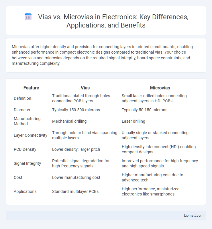
Microvias offer higher density and precision for connecting layers in printed circuit boards, enabling enhanced performance in compact electronic designs compared to traditional vias. Your choice between vias and microvias depends on the required signal integrity, board space constraints, and manufacturing complexity.
Table of Comparison
| Feature | Vias | Microvias |
|---|---|---|
| Definition | Traditional plated through holes connecting PCB layers | Small laser-drilled holes connecting adjacent layers in HDI PCBs |
| Diameter | Typically 150-500 microns | Typically 50-150 microns |
| Manufacturing Method | Mechanical drilling | Laser drilling |
| Layer Connectivity | Through-hole or blind vias spanning multiple layers | Usually single or stacked connecting adjacent layers |
| PCB Density | Lower density; larger pitch | High density interconnect (HDI) enabling compact designs |
| Signal Integrity | Potential signal degradation for high-frequency signals | Improved performance for high-frequency and high-speed signals |
| Cost | Lower manufacturing cost | Higher manufacturing cost due to advanced tech |
| Applications | Standard multilayer PCBs | High-performance, miniaturized electronics like smartphones |
Introduction to Vias and Microvias
Vias are vertical interconnect accesses used in printed circuit boards (PCBs) to establish electrical connections between different layers. Microvias are a subtype of vias with significantly smaller diameters, typically less than 150 micrometers, enabling higher component density and improved signal integrity in advanced PCB designs. The use of microvias is critical in high-frequency applications and multi-layer PCBs where space optimization and electrical performance are essential.
Key Differences Between Vias and Microvias
Vias are larger plated holes that electrically connect different layers of a printed circuit board (PCB), typically ranging from 150 to 500 microns in diameter, while microvias are significantly smaller, usually less than 150 microns, designed for high-density interconnects in advanced PCBs. Microvias are created using laser drilling technology, enabling finer pitch and higher layer counts compared to mechanically drilled vias. The key differences lie in size, manufacturing process, and application, with microvias offering improved electrical performance and space-saving benefits in compact electronic devices.
Types of Vias in PCB Design
Through-hole vias, blind vias, and buried vias are the primary types of vias used in PCB design, each serving distinct purposes in electrical connectivity and layer interconnection. Microvias, typically laser-drilled and less than 150 microns in diameter, enable high-density interconnections between adjacent layers without penetrating the entire board, optimizing space and signal integrity. Your choice between traditional vias and microvias impacts board complexity, manufacturing cost, and overall circuit performance.
What are Microvias?
Microvias are tiny vias used in printed circuit boards (PCBs) to create electrical connections between different layers with diameters typically less than 150 microns. They are formed using laser drilling techniques, allowing for higher-density interconnects and improved signal integrity in compact electronic designs. Your PCB designs benefit from microvias by enabling increased circuit complexity and enhanced performance in advanced electronic applications.
Advantages of Using Microvias
Microvias offer significant advantages in printed circuit board (PCB) design, including higher circuit density and improved electrical performance due to their smaller size and shorter depth compared to traditional vias. They enable finer pitch routing and reduce signal inductance and resistance, enhancing high-frequency signal integrity. The use of microvias also supports multi-layer PCB stacking, leading to more compact and lightweight electronic devices.
Limitations of Traditional Vias
Traditional vias face limitations such as larger diameters and increased drill depth requirements, restricting miniaturization on high-density PCBs. Their substantial size can cause signal integrity issues and limit routing complexity, impacting overall circuit performance. Your designs may benefit from microvias, which offer precision and improved electrical characteristics in compact layouts.
Applications of Vias vs Microvias
Vias are widely used in standard multilayer printed circuit boards (PCBs) for connecting different layers in high-power and high-frequency applications such as automotive electronics, industrial controls, and consumer devices. Microvias are essential in high-density interconnect (HDI) PCBs, supporting compact devices like smartphones, tablets, and aerospace electronics by enabling finer trace spacing and improved signal integrity. The choice between vias and microvias depends on factors including board complexity, space constraints, and electrical performance requirements.
Manufacturing Techniques for Vias and Microvias
Vias are typically manufactured using mechanical drilling, where holes are precisely drilled through multiple PCB layers, ensuring reliable electrical connections. Microvias, by contrast, are created using laser drilling techniques, allowing for much smaller and more precise holes that connect only adjacent layers, essential for high-density interconnects in advanced electronics. Choosing the right manufacturing technique for your PCB design affects both the performance and complexity of the final product, emphasizing precision and layer alignment.
Cost Considerations: Vias vs Microvias
Cost considerations between vias and microvias significantly impact printed circuit board (PCB) manufacturing budgets. Vias, typically larger and easier to produce, offer lower fabrication costs and are suitable for less dense designs. Microvias require advanced laser drilling technology, increasing production expenses, but enable higher circuit densities and improved electrical performance, which can justify the investment for compact, high-performance applications. Your choice should balance manufacturing costs with the desired board complexity and performance.
Future Trends in PCB Vias and Microvias
Future trends in PCB vias and microvias emphasize increased adoption of microvias for higher circuit density and improved signal integrity in compact electronic devices. Advances in laser drilling technology and materials enable finer microvias with enhanced reliability and thermal management, supporting the demands of 5G, IoT, and high-speed computing applications. Your PCBs will benefit from these developments by achieving greater performance, miniaturization, and design flexibility in next-generation electronics.
Vias vs Microvias Infographic