A ground plane provides a common reference point for all circuit components, minimizing noise and electromagnetic interference, while a power plane distributes stable voltage levels across the PCB. Ensuring proper separation and layout of your ground and power planes is crucial for optimizing signal integrity and overall circuit performance.
Table of Comparison
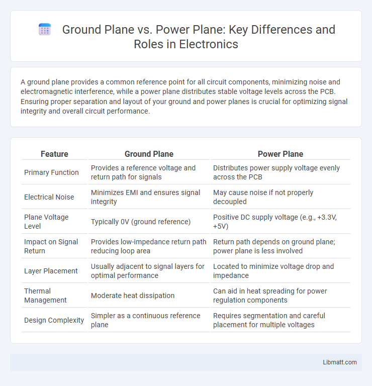
| Feature | Ground Plane | Power Plane |
|---|---|---|
| Primary Function | Provides a reference voltage and return path for signals | Distributes power supply voltage evenly across the PCB |
| Electrical Noise | Minimizes EMI and ensures signal integrity | May cause noise if not properly decoupled |
| Plane Voltage Level | Typically 0V (ground reference) | Positive DC supply voltage (e.g., +3.3V, +5V) |
| Impact on Signal Return | Provides low-impedance return path reducing loop area | Return path depends on ground plane; power plane is less involved |
| Layer Placement | Usually adjacent to signal layers for optimal performance | Located to minimize voltage drop and impedance |
| Thermal Management | Moderate heat dissipation | Can aid in heat spreading for power regulation components |
| Design Complexity | Simpler as a continuous reference plane | Requires segmentation and careful placement for multiple voltages |
Introduction to Ground Plane and Power Plane
A ground plane serves as a common reference point for all electrical circuits, providing a low-impedance path to reduce noise and signal interference in PCB design. Power planes deliver stable voltage levels to components, ensuring efficient power distribution and minimizing voltage drops across the board. Both planes play a crucial role in maintaining signal integrity and enhancing overall circuit performance.
Definitions: What Are Ground Plane and Power Plane?
A ground plane is a large conductive surface in a printed circuit board (PCB) used to provide a common reference point for all electrical signals, minimizing electromagnetic interference and ensuring signal integrity. A power plane is a dedicated conductive layer designed to distribute electrical power uniformly across the PCB, supplying stable voltage to various components. Both planes are essential for effective power management and noise reduction in electronic circuit design.
Core Functions of Ground and Power Planes
Ground planes provide a stable reference voltage for electronic circuits, minimizing noise and electromagnetic interference to ensure signal integrity. Power planes deliver consistent voltage levels to components, supporting efficient current distribution and reducing voltage drops across the PCB. Understanding these core functions helps optimize your circuit design for reliability and performance.
Importance in PCB Design
Ground planes and power planes are critical in PCB design for ensuring signal integrity and reducing electromagnetic interference (EMI). Ground planes provide a low-impedance return path that minimizes noise and crosstalk, while power planes deliver stable voltage levels and help distribute current efficiently across the board. Proper separation and layering of ground and power planes enhance thermal management and improve overall circuit performance.
Signal Integrity: Ground Plane vs Power Plane
A ground plane provides a stable reference voltage and return path for signals, minimizing noise and ensuring low impedance, which is critical for maintaining signal integrity. Power planes distribute voltage evenly but can introduce noise coupling if not properly decoupled, potentially degrading signal quality. For your PCB design, prioritizing a solid ground plane beneath signal layers helps reduce electromagnetic interference and preserves signal integrity more effectively than relying solely on power planes.
Electromagnetic Interference (EMI) Considerations
Ground planes significantly reduce electromagnetic interference (EMI) by providing a low-impedance path for return currents and minimizing loop areas that cause radiated emissions. Power planes, while essential for stable voltage distribution, can generate EMI if not properly decoupled or segmented, allowing noise currents to couple into sensitive circuits. Optimizing PCB stack-up with continuous ground planes beneath power planes effectively mitigates EMI by enhancing shielding and reducing crosstalk between high-frequency signals.
Power Distribution Network (PDN) Impacts
Ground planes and power planes play critical roles in the Power Distribution Network (PDN) by managing noise and ensuring stable voltage levels across electronic circuits. Ground planes provide a low-impedance return path that reduces electromagnetic interference (EMI) and enhances signal integrity, while power planes deliver consistent voltage with minimal voltage drop and inductance, crucial for high-frequency and high-current applications. Effective PDN design balances the interaction between ground and power planes to minimize voltage fluctuations, improve transient response, and support reliable device operation.
Design Guidelines for Ground and Power Planes
Design guidelines for ground and power planes emphasize minimizing impedance by using continuous, unbroken planes to ensure efficient current return paths and reduce electromagnetic interference (EMI). Proper separation between ground and power planes is critical, with careful stacking order to enhance signal integrity and thermal management in multilayer PCB designs. Additionally, placing decoupling capacitors close to power pins and maintaining low-inductance connections improve noise suppression and voltage stability across the power distribution network.
Common Mistakes and How to Avoid Them
Common mistakes when designing Ground Plane vs Power Plane include improper separation that leads to noise coupling and signal integrity issues. Failing to maintain continuous ground planes under high-speed signals can cause return current loops, increasing electromagnetic interference (EMI). To avoid these errors, ensure proper layer stacking with dedicated, unbroken ground and power planes and keep your layout consistent with the PCB manufacturer's design rules.
Best Practices for Optimizing Ground and Power Planes
Optimizing ground and power planes involves minimizing impedance and noise coupling by ensuring continuous, unbroken copper areas to maintain signal integrity and reduce electromagnetic interference. You should place the ground plane as close as possible to the power plane, using thin dielectric layers to enhance decoupling capacitance and improve power distribution. Strategic placement of vias and careful layer stacking further enhance return current paths and minimize voltage drops, enabling your PCB design to achieve optimal electrical performance.
Ground Plane vs Power Plane Infographic