P-type semiconductors contain an abundance of holes, which act as positive charge carriers, created by doping the material with elements that have fewer electrons than the semiconductor itself. N-type semiconductors have extra electrons as negative charge carriers, introduced by doping with elements that have more electrons, directly influencing Your device's electrical conductivity and behavior.
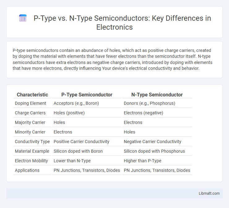
Table of Comparison
| Characteristic | P-Type Semiconductor | N-Type Semiconductor |
|---|---|---|
| Doping Element | Acceptors (e.g., Boron) | Donors (e.g., Phosphorus) |
| Charge Carriers | Holes (positive) | Electrons (negative) |
| Majority Carrier | Holes | Electrons |
| Minority Carrier | Electrons | Holes |
| Conductivity Type | Positive Carrier Conductivity | Negative Carrier Conductivity |
| Material Example | Silicon doped with Boron | Silicon doped with Phosphorus |
| Electron Mobility | Lower than N-Type | Higher than P-Type |
| Applications | PN Junctions, Transistors, Diodes | PN Junctions, Transistors, Diodes |
Introduction to Semiconductors
Semiconductors are materials with electrical conductivity between conductors and insulators, crucial for electronic devices. P-type semiconductors have positive charge carriers called holes, created by doping with elements like boron, while n-type semiconductors contain negative charge carriers, electrons, introduced by doping with elements such as phosphorus. Understanding the difference between p-type and n-type materials is essential for designing transistors, diodes, and integrated circuits that form the foundation of modern electronics.
What is a P-Type Semiconductor?
A P-type semiconductor is created by doping an intrinsic semiconductor, such as silicon, with trivalent elements like boron, which introduce holes as majority charge carriers. These holes act as positive charge carriers, enabling electrical conductivity by accepting electrons from neighboring atoms. Your electronic devices rely on P-type semiconductors to form the crucial junctions in diodes and transistors, allowing controlled flow of current.
What is an N-Type Semiconductor?
An N-type semiconductor is a material doped with pentavalent impurities such as phosphorus or arsenic, which introduce extra electrons as majority charge carriers. These free electrons enhance the electrical conductivity by providing negative charge carriers that move easily through the crystal lattice. N-type semiconductors are essential components in electronic devices like diodes, transistors, and integrated circuits due to their ability to conduct current efficiently.
Key Differences Between P-Type and N-Type Semiconductors
P-type semiconductors are created by doping intrinsic semiconductors with trivalent impurities, resulting in an abundance of positive charge carriers called holes, whereas n-type semiconductors are doped with pentavalent impurities, providing excess electrons as negative charge carriers. The electrical conductivity in p-type materials is primarily due to hole mobility, while in n-type materials, electron mobility dominates, affecting device performance and applications. These fundamental differences in charge carrier types and mobility are critical for designing semiconductor devices like diodes, transistors, and integrated circuits.
Charge Carriers: Holes vs Electrons
P-type semiconductors have holes as the majority charge carriers created by doping with elements that have fewer valence electrons, enabling them to accept electrons. N-type semiconductors feature electrons as the majority charge carriers due to doping with elements possessing extra valence electrons, supplying additional free electrons. Understanding the difference in charge carriers between holes in p-type and electrons in n-type materials is essential for optimizing your electronic device performance.
Doping Elements in P-Type and N-Type Materials
P-type semiconductors are created by doping intrinsic silicon with trivalent elements such as boron, aluminum, or gallium, which introduce holes as the majority charge carriers. N-type semiconductors result from doping silicon with pentavalent elements like phosphorus, arsenic, or antimony, contributing excess electrons as majority carriers. The choice of doping elements directly influences the electrical conductivity and charge carrier concentration in semiconductor devices.
Electrical Conductivity Comparison
P-type semiconductors have higher hole concentration, resulting in positive charge carriers that facilitate electrical conductivity through hole mobility. N-type semiconductors possess extra electrons as majority carriers, offering generally higher electrical conductivity due to electron mobility being greater than hole mobility. The intrinsic conductivity depends on dopant levels, with n-type materials typically exhibiting superior conductivity compared to p-type counterparts under similar doping conditions.
Applications of P-Type Semiconductors
P-type semiconductors are widely used in electronic devices such as diodes, transistors, and photovoltaic cells due to their positive charge carriers (holes). Their role in creating p-n junctions is crucial for the operation of integrated circuits and solar panels, enhancing device efficiency and performance. Understanding the applications of p-type materials can help you optimize semiconductor technology in various electronic and energy systems.
Applications of N-Type Semiconductors
N-type semiconductors are widely used in electronics due to their high electron mobility, essential for components like diodes, transistors, and integrated circuits. They serve as the foundation for n-channel MOSFETs, which are critical in digital logic circuits and power electronics. In solar cells, n-type materials enhance efficiency by providing better electron transport and reducing recombination losses.
P-Type vs N-Type: Role in Electronic Devices
P-type semiconductors, doped with elements like boron, create holes acting as positive charge carriers, crucial for forming the anode side of devices such as diodes and transistors. N-type semiconductors, doped with phosphorus or arsenic, provide free electrons as negative charge carriers essential for the cathode side and enhancing conductivity in electronic circuits. Your devices rely on the controlled interaction between p-type and n-type materials to enable efficient electron flow and switching functions in modern electronics.
p-type vs n-type Semiconductor Infographic