Thermal vias improve heat dissipation by connecting PCB layers directly to a heat source, while blind vias only connect outer layers to inner layers without passing through the entire board. Your choice depends on thermal management needs versus space-saving and signal integrity requirements.
Table of Comparison
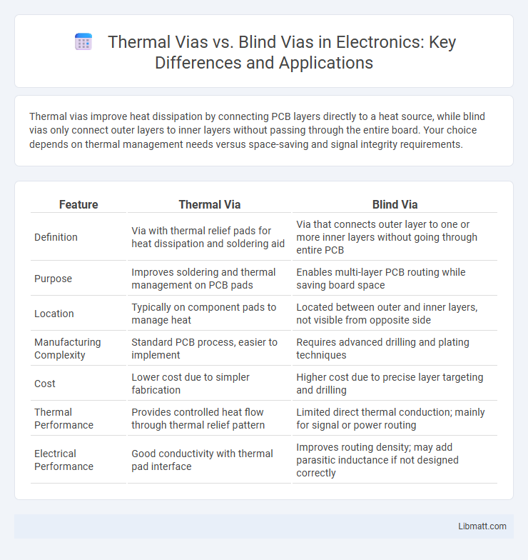
| Feature | Thermal Via | Blind Via |
|---|---|---|
| Definition | Via with thermal relief pads for heat dissipation and soldering aid | Via that connects outer layer to one or more inner layers without going through entire PCB |
| Purpose | Improves soldering and thermal management on PCB pads | Enables multi-layer PCB routing while saving board space |
| Location | Typically on component pads to manage heat | Located between outer and inner layers, not visible from opposite side |
| Manufacturing Complexity | Standard PCB process, easier to implement | Requires advanced drilling and plating techniques |
| Cost | Lower cost due to simpler fabrication | Higher cost due to precise layer targeting and drilling |
| Thermal Performance | Provides controlled heat flow through thermal relief pattern | Limited direct thermal conduction; mainly for signal or power routing |
| Electrical Performance | Good conductivity with thermal pad interface | Improves routing density; may add parasitic inductance if not designed correctly |
Introduction to Thermal Vias and Blind Vias
Thermal vias are designed to enhance heat dissipation in printed circuit boards (PCBs) by creating a pathway for heat to transfer from one layer to another, typically connecting heat-generating components to internal or external ground planes. Blind vias are PCB interconnects that connect an outer layer to one or more inner layers without passing through the entire board thickness, helping to save space and improve signal integrity in high-density designs. Both via types play crucial roles in optimizing thermal management and electrical performance in multilayer PCB fabrication.
Definitions: What are Thermal Vias vs Blind Vias?
Thermal vias are specialized PCB holes designed to efficiently dissipate heat from high-power components by connecting the top layer to inner or bottom layers with multiple small vias around a thermal pad. Blind vias are PCB holes that connect an outer layer to one or more inner layers without going through the entire board, optimizing space and signal integrity in multi-layer designs. Your choice between thermal vias and blind vias depends on heat management needs and board layout complexity.
Construction and Design Differences
Thermal vias feature a donut-shaped copper pad surrounding the hole, designed to improve heat dissipation while minimizing soldering issues, whereas blind vias connect outer layers to inner layers without penetrating the entire board, enhancing signal integrity and reducing board size. The construction of thermal vias emphasizes heat transfer with strategically spaced pads and annular rings, while blind vias require precise drilling and plating for reliable electrical connections between specific layers. Understanding these design differences helps you optimize PCB performance by balancing thermal management and electrical routing needs.
Applications in PCB Manufacturing
Thermal vias are commonly used in PCB manufacturing to enhance heat dissipation by connecting a component pad to internal or external copper planes, making them ideal for high-power applications such as LED boards and power electronics. Blind vias connect outer layers to one or more inner layers without going through the entire board, saving space and improving signal integrity in multilayer PCBs used in compact devices like smartphones and aerospace electronics. Your choice between thermal vias and blind vias depends on thermal management needs and design complexity in specific PCB applications.
Thermal Management: Role of Thermal Vias
Thermal vias play a crucial role in enhancing heat dissipation by providing a direct path for thermal energy from heat-generating components to the PCB's inner or outer layers, thus preventing overheating and improving reliability. In contrast, blind vias, which connect outer layers to one or more inner layers without going through the entire board, primarily serve electrical connectivity and offer limited thermal management benefits. Efficient thermal management in high-power electronic devices relies predominantly on thermal vias to maintain optimal operating temperatures and extend component lifespan.
Space Optimization: Advantage of Blind Vias
Blind vias offer superior space optimization compared to thermal vias by occupying less area on the PCB surface while maintaining reliable electrical connections between inner layers. Their design reduces the need for extensive clearance and allows for higher component density on your circuit board. This makes blind vias especially advantageous in compact electronic devices where efficient use of space is critical.
Cost Factors and Manufacturing Complexity
Thermal vias typically incur higher manufacturing costs due to their precise plating process and the need for thermal pads, increasing production complexity. Blind vias, which connect outer layers to one or more inner layers without passing through the entire board, require advanced drilling and plating techniques, significantly raising fabrication expenses. Cost factors for thermal vias hinge on enhanced heat dissipation requirements, whereas blind vias demand specialized equipment and tighter process control, impacting overall PCB manufacturing complexity.
Reliability and Performance Considerations
Thermal vias enhance reliability by efficiently dissipating heat away from high-power components, reducing thermal stress and improving long-term performance in multilayer PCBs. Blind vias, which connect outer layers to one or more inner layers without passing through the entire board, minimize signal loss and crosstalk, offering better electrical performance in high-speed applications. Choosing between thermal and blind vias depends on balancing thermal management needs with signal integrity requirements in complex PCB designs.
Industry Standards and Best Practices
Thermal vias adhere to IPC standards such as IPC-2221 and IPC-2152, optimizing heat dissipation by surrounding the via barrel with a heat-resistant pad. Blind vias, compliant with IPC-6012 and IPC-4761, offer efficient layer-to-layer connectivity without passing through the entire PCB, saving space and improving signal integrity. Your PCB design should follow these industry best practices to ensure manufacturability and performance reliability.
Choosing Between Thermal Vias and Blind Vias
Choosing between thermal vias and blind vias depends heavily on the specific requirements of heat dissipation and circuit density in PCB design. Thermal vias are optimized for enhancing heat transfer from heat-generating components to internal or external copper planes, improving thermal management in high-power applications. Blind vias, by contrast, provide efficient electrical connections between outer and inner layers without passing through the entire board, which conserves space and reduces parasitic capacitance, making them ideal for high-density, multilayer PCB designs.
Thermal via vs Blind via Infographic