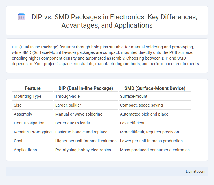
DIP (Dual Inline Package) features through-hole pins suitable for manual soldering and prototyping, while SMD (Surface-Mount Device) packages are compact, mounted directly onto the PCB surface, enabling higher component density and automated assembly. Choosing between DIP and SMD depends on Your project's space constraints, manufacturing methods, and performance requirements.
Table of Comparison
| Feature | DIP (Dual In-line Package) | SMD (Surface-Mount Device) |
|---|---|---|
| Mounting Type | Through-hole | Surface-mount |
| Size | Larger, bulkier | Compact, space-saving |
| Assembly | Manual or wave soldering | Automated pick-and-place |
| Heat Dissipation | Better due to leads | Less efficient |
| Repair & Prototyping | Easier to handle and replace | More difficult, requires precision |
| Cost | Higher per unit for small volumes | Lower per unit in mass production |
| Applications | Prototyping, hobby electronics | Mass-produced consumer electronics |
Introduction to DIP and SMD Packages
DIP (Dual In-line Package) features through-hole mounting with two parallel rows of pins, commonly used for prototyping and easy manual soldering. SMD (Surface-Mount Device) packages are designed for surface mounting directly onto PCB pads, enabling higher component density and automated assembly. Your choice between DIP and SMD affects manufacturing processes, circuit design, and overall device size.
Historical Overview of DIP and SMD Technologies
DIP (Dual In-line Package) technology emerged in the 1960s as one of the first standardized methods for mounting integrated circuits on printed circuit boards, characterized by its two parallel rows of pins for through-hole soldering. SMD (Surface-Mount Device) technology evolved in the 1980s, driven by the demand for miniaturization and automated assembly, featuring components directly mounted onto the PCB surface without lead insertion. Your choice between DIP and SMD packages impacts assembly techniques, board space, and component density, reflecting the technological advances from bulky to compact electronic design.
Structural Differences Between DIP and SMD
Dual In-Line Package (DIP) features two parallel rows of through-hole pins designed for insertion into PCB holes, offering robust mechanical stability and ease of manual soldering. Surface-Mount Device (SMD) packages have flat, short leads or terminations that are soldered directly onto the PCB surface, enabling higher component density and automated assembly processes. The structural difference lies in DIP's through-hole pins versus SMD's flat contact points, influencing board layout, manufacturing techniques, and electrical performance.
Assembly and Mounting Process
DIP (Dual In-line Package) components require through-hole mounting, where pins are inserted into drilled holes on the PCB and soldered, offering robust mechanical strength ideal for prototyping and manual assembly. SMD (Surface-Mount Device) packages are mounted directly onto the surface of the PCB pads, enabling automated pick-and-place assembly with higher component density and faster production rates. The SMD process involves solder reflow techniques, reducing lead bending and improving electrical performance, while DIP requires more labor-intensive soldering and space.
Size and Space Efficiency Comparison
DIP (Dual In-line Package) components have larger dimensions and require more board space due to their through-hole mounting design, making them less suitable for compact electronic devices. In contrast, SMD (Surface-Mount Device) packages offer significantly smaller sizes and improved space efficiency by mounting directly onto the PCB surface, enabling higher component density. Your choice between DIP and SMD should consider available board space and design complexity, with SMD being preferred for miniaturized and high-density circuits.
Performance and Electrical Characteristics
DIP (Dual In-line Package) components generally exhibit higher lead inductance and parasitic capacitance, which can impact high-frequency performance and signal integrity compared to SMD (Surface-Mount Device) packages. SMD packages offer lower electrical parasitics, resulting in improved high-frequency response and reduced signal distortion, making them preferable for high-speed and high-frequency electronic applications. The compact size and closer lead spacing of SMD devices also contribute to enhanced thermal performance and lower electrical resistance, optimizing overall circuit efficiency.
Applications of DIP vs SMD Packages
DIP (Dual In-line Package) components are widely used in prototyping, through-hole mounting, and applications requiring easy manual soldering or replacement, such as in educational kits and vintage electronics. SMD (Surface-Mount Device) packages dominate modern, high-density circuit designs due to their smaller size and compatibility with automated assembly processes, making them ideal for smartphones, laptops, and compact consumer electronics. Your choice between DIP and SMD packages depends on factors like production volume, device complexity, and repairability requirements.
Cost and Manufacturing Considerations
DIP (Dual In-line Package) components generally have higher manufacturing costs due to larger size and through-hole mounting processes, which require more complex PCB drilling and soldering steps compared to SMD (Surface-Mount Device) packages. SMD packages enable automated, high-speed assembly with lower labor costs and reduced material usage, leading to overall cost efficiency in mass production. The compact size of SMD components also allows for smaller PCB designs, minimizing material costs and enhancing manufacturing throughput.
Pros and Cons of DIP and SMD Packages
DIP (Dual In-line Package) offers easy manual handling and straightforward prototyping, making it ideal for beginners and through-hole circuit designs, but it occupies more board space and has limited high-frequency performance. SMD (Surface-Mount Device) packages provide compact size, higher component density, and better electrical performance suitable for automated assembly processes, although they require precise soldering techniques and are less repair-friendly. Your choice depends on the application's space constraints, production volume, and assembly capabilities.
Future Trends in Electronic Packaging
Future trends in electronic packaging emphasize the shift from traditional DIP (Dual In-line Package) to advanced SMD (Surface-Mount Device) technologies due to their superior performance, miniaturization, and enhanced thermal management. SMD packages enable higher circuit density, better signal integrity, and compatibility with automated assembly processes, making them essential for next-generation electronics. Your designs will benefit from adopting SMD as it supports faster production cycles and improved reliability in increasingly compact and complex devices.
DIP vs SMD Package Infographic