Solder mask protects your PCB's copper traces from oxidation and prevents solder bridges during assembly by covering areas not meant for soldering, while silkscreen provides essential visual information such as component labels and part outlines for easier identification and troubleshooting. Choosing the right combination enhances both the durability and usability of your electronic boards.
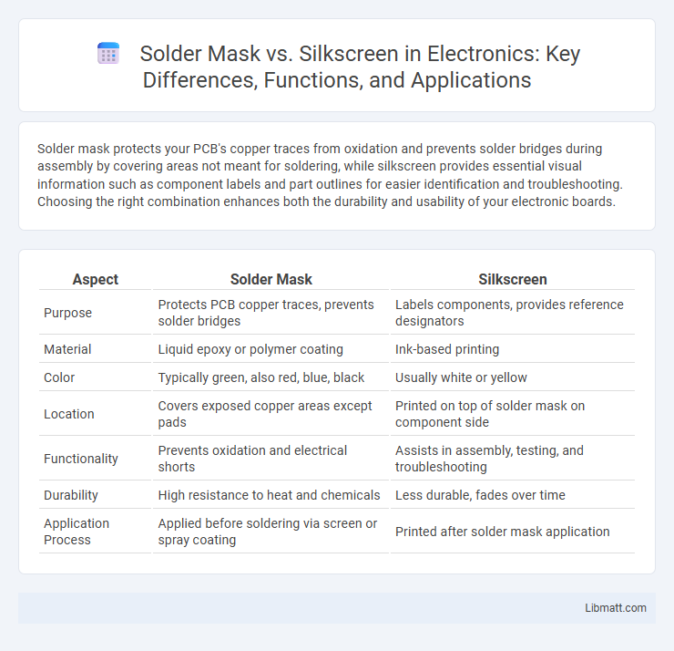
Table of Comparison
| Aspect | Solder Mask | Silkscreen |
|---|---|---|
| Purpose | Protects PCB copper traces, prevents solder bridges | Labels components, provides reference designators |
| Material | Liquid epoxy or polymer coating | Ink-based printing |
| Color | Typically green, also red, blue, black | Usually white or yellow |
| Location | Covers exposed copper areas except pads | Printed on top of solder mask on component side |
| Functionality | Prevents oxidation and electrical shorts | Assists in assembly, testing, and troubleshooting |
| Durability | High resistance to heat and chemicals | Less durable, fades over time |
| Application Process | Applied before soldering via screen or spray coating | Printed after solder mask application |
Introduction to PCB Layers
The solder mask is a protective layer applied on printed circuit boards (PCBs) to prevent solder bridges and protect copper traces from oxidation. Silkscreen, on the other hand, is a non-conductive layer used to print component designators, logos, and other reference information on the PCB surface. Together, these layers enhance PCB functionality by improving assembly accuracy and ensuring durability during operation.
What is a Solder Mask?
A solder mask is a protective layer applied to printed circuit boards (PCBs) that prevents solder bridging and corrosion while enhancing electrical insulation. It is typically a polymer-based coating that covers the copper traces except for the areas where soldering occurs. The solder mask improves the durability and reliability of PCBs by shielding circuits from environmental contaminants and mechanical wear.
What is a Silkscreen?
A silkscreen is a layer of ink applied to the surface of a printed circuit board (PCB) that provides labels, symbols, and component identifiers to aid in assembly and troubleshooting. Unlike the solder mask, which protects the copper traces from oxidation and prevents solder bridges, the silkscreen enhances the board's visual clarity and usability by marking pin numbers, test points, and polarity indicators. Your PCB design relies on silkscreen accuracy to ensure proper component placement and efficient manufacturing processes.
Key Functions: Solder Mask vs Silkscreen
Solder mask primarily functions as a protective layer that prevents solder bridging and environmental damage on printed circuit boards (PCBs), ensuring electrical insulation between conductive traces. Silkscreen serves to provide clear, legible markings such as component identifiers, logos, and symbols, aiding in assembly, troubleshooting, and maintenance. Both layers are crucial for PCB functionality, with solder mask enhancing reliability and silkscreen improving readability.
Material Composition and Application
Solder mask is primarily composed of epoxy liquid and resin-based materials designed to protect printed circuit boards (PCBs) from oxidation and prevent solder bridges during assembly. Silkscreen utilizes ink made from epoxy, acrylic, or UV-curable materials to print component labels, symbols, and identification markers on PCB surfaces. The solder mask is applied as a protective coating over copper traces, whereas silkscreen is printed on top of the solder mask for visual aids and assembly guidance.
Visual Differences and Identification
Solder mask is a colored protective layer, typically green, covering the PCB to prevent solder bridging and oxidation, while silkscreen is a white or light-colored printed layer that displays component labels, symbols, and reference designators. You can identify solder mask by its smooth, solid-colored finish that covers most of the PCB surface, whereas silkscreen appears as crisp, text and graphic markings printed on top of the solder mask. Visual differentiation is critical during PCB assembly and inspection to ensure proper component placement and avoid shorts.
Importance in PCB Manufacturing
The solder mask is crucial in PCB manufacturing as it prevents solder bridges and protects copper traces from oxidation and contamination, ensuring electrical isolation and device reliability. Silkscreen provides essential component identification, orientation, and assembly instructions, enhancing the accuracy of component placement and troubleshooting. Together, these layers improve the overall quality, durability, and functionality of printed circuit boards.
Common Issues and Defects
Solder mask defects such as pinholes, bridging, and peeling often cause short circuits and soldering difficulties, compromising PCB reliability. Silkscreen issues include smudging, misalignment, and fading, which affect component identification and assembly accuracy. Ensuring proper application and material compatibility helps you avoid these common problems and maintain PCB performance.
Cost Implications in PCB Design
Solder mask significantly reduces PCB manufacturing costs by preventing solder bridges and reducing rework, whereas silkscreen primarily adds minimal cost for labeling and component identification. Your choice of solder mask color and type can impact overall expenses, with green solder mask being the most cost-effective option. Investing in a quality solder mask upfront helps avoid costly defects, while silkscreen costs remain relatively low and consistent across designs.
Choosing Between Solder Mask and Silkscreen
Choosing between solder mask and silkscreen depends on their distinct roles in PCB manufacturing; solder mask protects copper traces from oxidation and prevents solder bridges during assembly, while silkscreen provides essential component identification and assembly instructions. Your decision should consider whether the primary need is electrical insulation and protection or visual guidance for component placement. For optimal PCB performance and ease of assembly, balancing the coverage of solder mask with clear, legible silkscreen markings is key.
Solder mask vs Silkscreen Infographic