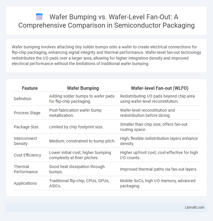
Wafer bumping involves attaching tiny solder bumps onto a wafer to create electrical connections for flip-chip packaging, enhancing signal integrity and thermal performance. Wafer-level fan-out technology redistributes the I/O pads over a larger area, allowing for higher integration density and improved electrical performance without the limitations of traditional wafer bumping.
Table of Comparison
| Feature | Wafer Bumping | Wafer-level Fan-out (WLFO) |
|---|---|---|
| Definition | Adding solder bumps to wafer pads for flip-chip packaging. | Redistributing I/O pads beyond chip area using wafer-level reconstitution. |
| Process Stage | Post-fabrication wafer bump metallization. | Wafer-level reconstitution and redistribution before dicing. |
| Package Size | Limited by chip footprint size. | Smaller than chip size; offers fan-out routing space. |
| Interconnect Density | Medium; constrained to bump pitch. | High; flexible redistribution layers enhance density. |
| Cost Efficiency | Lower initial cost; higher bumping complexity at finer pitches. | Higher upfront cost; cost-effective for high I/O counts. |
| Thermal Performance | Good heat dissipation through bumps. | Improved thermal paths via fan-out layers. |
| Applications | Traditional flip-chip, CPUs, GPUs, ASICs. | Mobile SoCs, high I/O memory, advanced packaging. |
Introduction to Wafer Bumping and Wafer-level Fan-out
Wafer bumping is a key semiconductor packaging technology that involves depositing metal bumps on wafer pads to enable electrical connections between the die and the substrate, enhancing signal integrity and thermal performance. Wafer-level fan-out (WLFO) integrates redistribution layers directly on the wafer, expanding I/O density and allowing for thinner, higher-performance packages without the need for traditional substrates. Both technologies play critical roles in advanced microelectronics by improving interconnect performance and supporting miniaturization trends in devices.
Historical Evolution of Advanced Packaging
Wafer bumping emerged as a pioneering technique in the 1980s, enabling reliable electrical connections in flip-chip technology and driving the miniaturization of semiconductor devices. Wafer-level fan-out (WLF) packaging evolved in the 2010s to address limitations in interconnect density and package footprint, offering improved performance through redistributed I/O and embedded redistribution layers. The historical progression from wafer bumping to WLF reflects a shift towards higher integration, enhanced thermal management, and increased scalability in advanced semiconductor packaging.
Core Principles of Wafer Bumping
Wafer bumping involves creating small conductive bumps on a wafer's surface to enable electrical and mechanical connections between the chip and the package, typically using solder or copper pillars. This process ensures precise alignment and robust interconnectivity, supporting high-density chip integration and improved electrical performance. In contrast, wafer-level fan-out redistributes I/O connections beyond the chip's footprint without the need for bumps at the initial level, relying instead on a build-up process to achieve increased integration and miniaturization.
Fundamentals of Wafer-level Fan-out Technology
Wafer-level fan-out (WLFO) technology enhances semiconductor packaging by redistributing I/O connections beyond the chip's original footprint, enabling higher integration density compared to traditional wafer bumping. This process involves embedding dies in a reconstituted wafer with an encapsulant, followed by creating fan-out redistribution layers that facilitate complex interconnect patterns. By leveraging WLFO, your devices achieve improved electrical performance, reduced package size, and cost-effective scalability for advanced applications.
Process Flow Comparison: Wafer Bumping vs Wafer-level Fan-out
Wafer bumping involves depositing solder bumps directly onto the wafer pads to enable flip-chip assembly, typically following wafer thinning and under-bump metallization steps, whereas wafer-level fan-out (WLF) extends the redistribution layer beyond the original die area to accommodate more I/O connections without the need for traditional bumps. The wafer bumping process flow emphasizes precise alignment and bump formation, while WLF integrates fan-out redistribution, encapsulation, and reconstitution before bumping. This fundamental difference in process flow leads to varied applications, with wafer bumping suited for high-density interconnects on standard dies and wafer-level fan-out enabling ultra-thin, high I/O packages with enhanced electrical performance.
Key Materials Used in Each Process
Wafer bumping primarily uses solder alloys such as tin-silver-copper (SAC) and lead-free solders to form the conductive bumps, while under-bump metallization (UBM) layers typically comprise nickel, copper, or gold for improved adhesion and conductivity. In wafer-level fan-out (WLO) technology, redistribution layers (RDLs) are fabricated using copper traces with dielectric materials like polyimide or epoxy-based polymers to enable the fan-out structure beyond the chip's original footprint. Both processes rely on precise deposition and plating materials to ensure reliable electrical connections and mechanical stability in advanced semiconductor packaging.
Performance and Reliability Differences
Wafer bumping typically offers superior electrical performance due to shorter interconnect lengths, resulting in lower resistance and capacitance, which enhances signal integrity and enables high-frequency applications. Wafer-level fan-out (WLFO) improves reliability by providing a redistribution layer that reduces stress and thermal mismatch between the die and the package, enhancing mechanical robustness and thermal management. WLFO also supports higher I/O density and scalability, offering a more flexible solution for heterogeneous integration despite slightly increased parasitic effects compared to traditional wafer bumping.
Cost Implications and Scalability
Wafer Bumping offers a cost-effective solution for standard IC packaging, leveraging mature processes that minimize per-unit expenses in high-volume production. Wafer-level Fan-out (WLF) provides enhanced scalability for complex, high-density interconnects but involves higher initial tooling and process development costs, impacting overall budget considerations. Assessing Your project volume and complexity helps determine which method balances cost efficiency and scalability demands most effectively.
Application Areas and Market Trends
Wafer bumping is widely used in traditional packaging applications such as flip-chip assembly and memory devices, offering reliable electrical connections for high-performance computing and consumer electronics. Wafer-level fan-out (WLFO) excels in advanced applications like 5G, IoT, and AI, enabling thinner, smaller, and more complex devices due to its ability to redistribute I/O pads beyond the chip boundary. Market trends indicate a growing preference for WLFO driven by demand for miniaturization and enhanced functionality, while wafer bumping remains integral in established semiconductor segments, maintaining a balanced coexistence in your manufacturing strategy.
Future Outlook: Emerging Innovations in Wafer-level Packaging
Emerging innovations in wafer-level packaging focus on improving scalability, electrical performance, and thermal management through advanced wafer bumping and wafer-level fan-out (WLFO) techniques. Next-generation materials like copper pillar bumps and redistribution layers enable finer pitch and higher density interconnections, supporting 5G, IoT, and AI applications. The integration of heterogeneous components within WLFO solutions promises enhanced miniaturization and cost-efficiency in semiconductor manufacturing's future landscape.
Wafer Bumping vs Wafer-level Fan-out Infographic