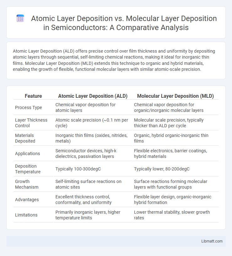
Atomic Layer Deposition (ALD) offers precise control over film thickness and uniformity by depositing atomic layers through sequential, self-limiting chemical reactions, making it ideal for inorganic thin films. Molecular Layer Deposition (MLD) extends this technique to organic and hybrid materials, enabling the growth of flexible, functional molecular layers with similar atomic-scale precision.
Table of Comparison
| Feature | Atomic Layer Deposition (ALD) | Molecular Layer Deposition (MLD) |
|---|---|---|
| Process Type | Chemical vapor deposition for atomic layers | Chemical vapor deposition for organic/inorganic molecular layers |
| Layer Thickness Control | Atomic scale precision (~0.1 nm per cycle) | Molecular scale precision, typically thicker than ALD per cycle |
| Materials Deposited | Inorganic thin films (oxides, nitrides, metals) | Organic, hybrid organic-inorganic thin films |
| Applications | Semiconductor devices, high-k dielectrics, passivation layers | Flexible electronics, barrier coatings, hybrid materials |
| Deposition Temperature | Typically 100-300degC | Typically lower, 80-200degC |
| Growth Mechanism | Self-limiting surface reactions on atomic sites | Surface reactions forming molecular layers with functional groups |
| Advantages | Excellent thickness control, conformality, and uniformity | Flexible layer design, organic-inorganic hybrid formation |
| Limitations | Primarily inorganic layers, higher temperature limits | Lower thermal stability, slower growth rates |
Introduction to Atomic Layer Deposition and Molecular Layer Deposition
Atomic Layer Deposition (ALD) and Molecular Layer Deposition (MLD) are advanced thin-film deposition techniques critical for nanotechnology and semiconductor manufacturing. ALD utilizes self-limiting chemical reactions to deposit atomic-scale layers of inorganic materials, ensuring exceptional uniformity and conformality on complex substrates. MLD, on the other hand, extends this approach to organic or hybrid organic-inorganic layers, enabling precise control over molecular architecture and film thickness at the nanoscale, making these methods complementary for fabricating multifunctional coatings and devices.
Fundamental Principles of Atomic Layer Deposition (ALD)
Atomic Layer Deposition (ALD) operates on self-limiting surface reactions that enable precise control over film thickness at the atomic scale, employing sequential exposure to gaseous precursors. The process involves alternating pulses of these precursors, which react on the substrate surface in a layer-by-layer fashion, ensuring uniformity and conformity even on complex nanostructures. Compared to Molecular Layer Deposition (MLD), ALD primarily deposits inorganic thin films, whereas MLD incorporates organic precursors for hybrid materials, making ALD essential for applications demanding high-quality oxide, nitride, or metal layers in semiconductor manufacturing and nanotechnology.
Core Mechanisms of Molecular Layer Deposition (MLD)
Molecular Layer Deposition (MLD) operates through sequential, self-limiting surface reactions involving organic precursors, enabling precise, molecular-scale film growth with excellent control over thickness and composition. Unlike Atomic Layer Deposition (ALD), which deposits inorganic layers atom-by-atom, MLD forms hybrid organic-inorganic films by alternating exposure to vapor-phase reactants that react with surface functional groups. Your ability to tailor surface chemistry at the molecular level using MLD supports advanced applications in flexible electronics, barrier coatings, and hybrid nanomaterials.
Process Differences Between ALD and MLD
Atomic Layer Deposition (ALD) involves the sequential exposure of surfaces to gaseous precursors, enabling atomic-level control in thin-film growth through self-limiting surface reactions. Molecular Layer Deposition (MLD) extends this principle by incorporating organic precursors, allowing for the formation of hybrid organic-inorganic thin films with molecular-level precision. The process differences lie in ALD's emphasis on inorganic atomic layers versus MLD's use of organic molecules, which impacts film composition, flexibility, and functional properties, crucial for tailoring Your coatings in advanced applications.
Material Types and Compatibility
Atomic Layer Deposition (ALD) excels in depositing inorganic materials like oxides, nitrides, and metals with exceptional conformality on complex surfaces, making it ideal for semiconductor and microelectronics applications. Molecular Layer Deposition (MLD) specializes in organic and hybrid organic-inorganic thin films, enabling deposition of polymers and flexible materials compatible with biomedical and flexible electronics. Your choice between ALD and MLD depends on the required material type and compatibility with substrate properties for optimal device performance.
Film Properties: Thickness, Uniformity, and Conformality
Atomic Layer Deposition (ALD) provides exceptional control over film thickness, achieving uniform layers at the atomic scale with unparalleled conformality on complex 3D structures. Molecular Layer Deposition (MLD) extends this precision to organic-inorganic hybrid films, enabling tunable thickness and enhanced flexibility while maintaining high uniformity and conformal coverage. Your choice between ALD and MLD depends on the desired film composition and application, with ALD excelling in dense inorganic films and MLD offering versatile hybrid material properties.
Application Areas for ALD and MLD Technologies
Atomic Layer Deposition (ALD) is widely utilized in semiconductor fabrication, energy storage devices, and corrosion-resistant coatings due to its ability to produce ultra-thin, conformal films with atomic-level precision. Molecular Layer Deposition (MLD) finds key applications in organic-inorganic hybrid materials, flexible electronics, and biomaterials, enabling the formation of tailored polymeric thin films with molecular-scale control. Both technologies advance nanotechnology by enabling precise film growth for next-generation microelectronics, optoelectronics, and protective functional layers.
Advantages and Limitations of ALD
Atomic Layer Deposition (ALD) offers exceptional thickness control, uniformity, and conformality on complex 3D structures, making it ideal for semiconductor and nanotechnology applications. However, ALD's limitations include slower deposition rates and higher equipment costs compared to other thin-film techniques, which can impact throughput and scalability. Your choice of ALD can significantly enhance material precision but requires consideration of process efficiency and economic factors.
Pros and Cons of MLD Compared to ALD
Molecular Layer Deposition (MLD) offers superior flexibility in incorporating organic and hybrid materials compared to Atomic Layer Deposition (ALD), enabling the fabrication of ultrathin, conformal films with tailored chemical functionalities. MLD's primary limitation lies in slower deposition rates and a narrower range of available precursors, impacting throughput and material diversity relative to ALD's extensively developed inorganic processes. While ALD excels in producing dense, uniform inorganic layers with high thermal stability, MLD's advantage is the ability to engineer hybrid interfaces and polymeric films essential for applications in flexible electronics and advanced coatings.
Future Trends in Layer-by-Layer Deposition Techniques
Future trends in layer-by-layer deposition techniques emphasize enhanced control over film thickness, uniformity, and conformality at the atomic scale. Atomic Layer Deposition (ALD) advances focus on expanding precursor libraries and plasma-enhanced processes to enable low-temperature, high-throughput manufacturing for semiconductor and energy devices. Molecular Layer Deposition (MLD) developments target hybrid organic-inorganic films with tunable mechanical and electronic properties, driving innovations in flexible electronics and advanced coatings.
Atomic Layer Deposition vs Molecular Layer Deposition Infographic