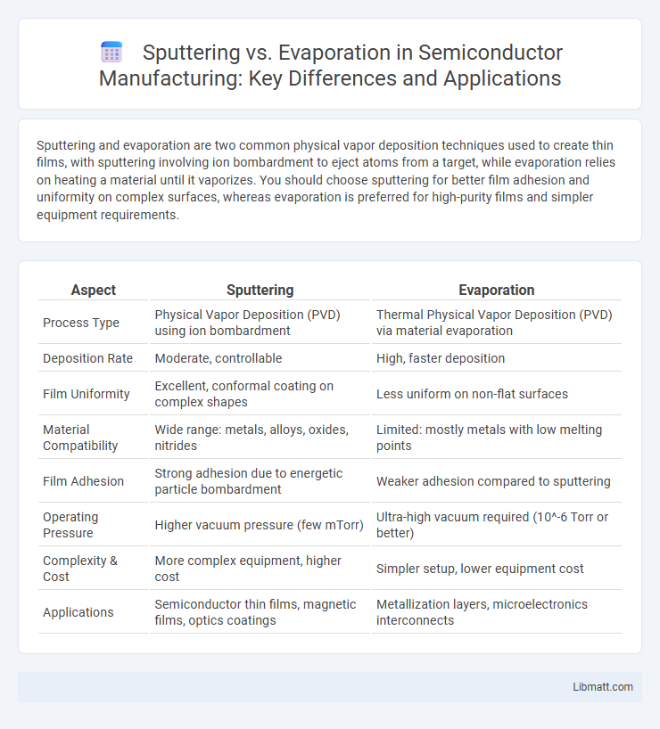
Sputtering and evaporation are two common physical vapor deposition techniques used to create thin films, with sputtering involving ion bombardment to eject atoms from a target, while evaporation relies on heating a material until it vaporizes. You should choose sputtering for better film adhesion and uniformity on complex surfaces, whereas evaporation is preferred for high-purity films and simpler equipment requirements.
Table of Comparison
| Aspect | Sputtering | Evaporation |
|---|---|---|
| Process Type | Physical Vapor Deposition (PVD) using ion bombardment | Thermal Physical Vapor Deposition (PVD) via material evaporation |
| Deposition Rate | Moderate, controllable | High, faster deposition |
| Film Uniformity | Excellent, conformal coating on complex shapes | Less uniform on non-flat surfaces |
| Material Compatibility | Wide range: metals, alloys, oxides, nitrides | Limited: mostly metals with low melting points |
| Film Adhesion | Strong adhesion due to energetic particle bombardment | Weaker adhesion compared to sputtering |
| Operating Pressure | Higher vacuum pressure (few mTorr) | Ultra-high vacuum required (10^-6 Torr or better) |
| Complexity & Cost | More complex equipment, higher cost | Simpler setup, lower equipment cost |
| Applications | Semiconductor thin films, magnetic films, optics coatings | Metallization layers, microelectronics interconnects |
Introduction to Thin Film Deposition Techniques
Thin film deposition techniques such as sputtering and evaporation are crucial for fabricating high-performance coatings in semiconductors, optics, and electronics. Sputtering involves ejecting material from a target using ionized gas, offering better film adhesion and uniformity, while evaporation relies on heating a source material until it vaporizes, providing high deposition rates and simplicity. Choosing the right method depends on your thin film requirements, including material compatibility, film thickness, and substrate sensitivity.
Understanding Sputtering: Principles and Process
Sputtering involves bombarding a target material with high-energy ions to eject atoms, which then deposit onto a substrate, creating thin films with excellent adhesion and uniformity. This physical vapor deposition technique relies on momentum transfer rather than thermal energy, making it suitable for materials with high melting points. Understanding sputtering helps optimize coating processes for your applications requiring precise control over film thickness and composition.
Evaporation Method: Fundamentals and Workflow
Evaporation is a physical vapor deposition (PVD) technique where a source material is heated in a vacuum chamber until it vaporizes, allowing atoms or molecules to condense on a substrate to form a thin film. The workflow of evaporation involves heating the material using resistive coils or electron beam sources, maintaining high vacuum conditions to reduce contamination, and controlling deposition rate and thickness for uniform coating. Your ability to precisely manage parameters such as temperature, vacuum level, and deposition rate ensures high-quality, adherent thin films for applications in optics, electronics, and coatings.
Equipment and Setup Requirements
Sputtering requires a vacuum chamber equipped with a gas supply, usually argon, and a target material cathode connected to a power source to ionize gas atoms for thin film deposition. Evaporation uses a vacuum chamber with a thermal evaporation source, such as a resistive heater or electron beam, to vaporize the source material, which then condenses on the substrate. Sputtering setups are typically more complex and expensive due to plasma generation and target cathode configuration, while evaporation systems offer simpler operation and lower initial costs but less uniform film coverage.
Material Compatibility and Versatility
Sputtering offers superior material compatibility, enabling deposition of metals, insulators, and alloys on diverse substrates with high uniformity and adhesion. Evaporation excels in depositing pure metals and organic materials but faces limitations with complex alloys and less uniform coverage on intricate surfaces. Your choice depends on the specific material requirements and substrate characteristics for achieving optimal thin film performance.
Film Quality: Adhesion, Uniformity, and Purity
Sputtering generally produces films with superior adhesion, uniformity, and purity compared to evaporation, due to its energetic ion bombardment that creates denser and more compact coatings. The process enables better control over film thickness and composition, enhancing uniformity across complex substrates and minimizing contamination. Your choice of sputtering will likely yield higher-quality films critical for advanced electronic and optical applications.
Deposition Rate and Process Efficiency
Sputtering offers a lower deposition rate compared to evaporation but provides superior process efficiency through enhanced film uniformity and adhesion. Evaporation achieves higher deposition rates with faster material deposition but often sacrifices film density and coverage consistency. Process efficiency in sputtering is improved by better target utilization and less material waste, making it ideal for complex or high-precision coatings.
Cost Analysis: Sputtering vs. Evaporation
Sputtering typically incurs higher initial equipment costs compared to evaporation due to its complex plasma generation and target handling systems. However, sputtering offers more uniform film thickness and better adhesion, potentially reducing material waste and rework expenses, making it cost-effective for high-precision applications. When evaluating your budget, consider evaporation's lower upfront costs but higher material usage and potential limitations in coating uniformity, which might increase long-term operational expenses.
Typical Applications and Industry Use Cases
Sputtering is extensively used in semiconductor manufacturing, data storage devices, and solar cells due to its ability to produce uniform thin films with excellent adhesion on complex surfaces. Evaporation finds typical applications in the production of optical coatings, decorative finishes, and microelectronics where high purity films and fast deposition rates are essential. Your choice between sputtering and evaporation depends on the specific industry requirements such as film quality, material type, and substrate compatibility.
Choosing the Right Technique: Key Considerations
Choosing the right thin-film deposition technique depends on factors like film adhesion, material type, and process temperature. Sputtering offers superior adhesion and uniformity for metals and alloys, while evaporation is ideal for organic materials and low melting point metals. Your decision should also consider equipment cost, vacuum requirements, and desired film thickness to optimize performance and efficiency.
Sputtering vs Evaporation Infographic