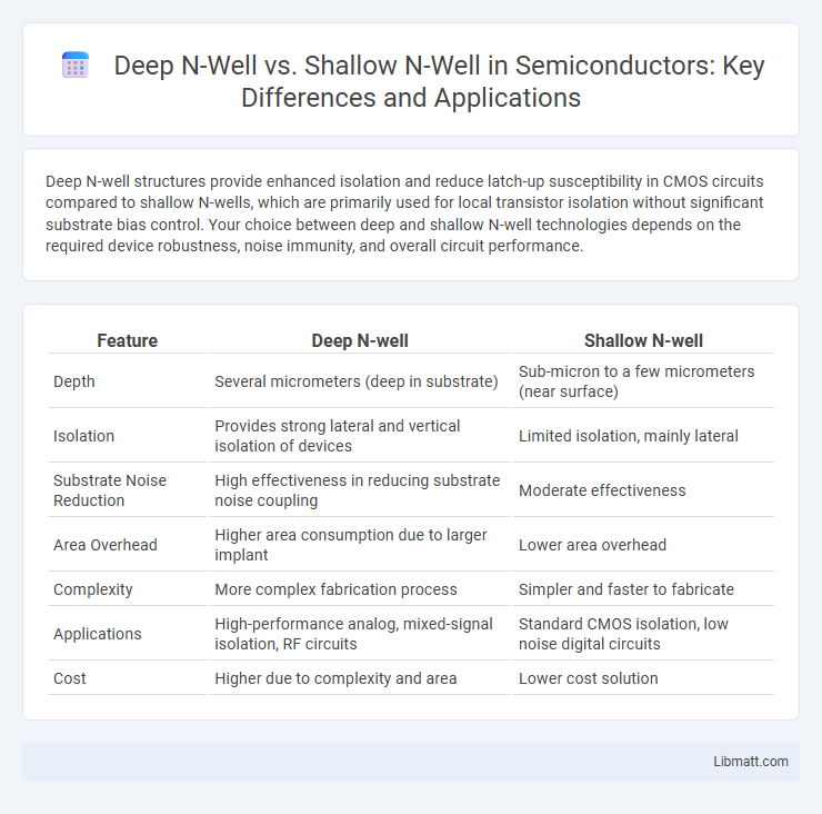
Deep N-well structures provide enhanced isolation and reduce latch-up susceptibility in CMOS circuits compared to shallow N-wells, which are primarily used for local transistor isolation without significant substrate bias control. Your choice between deep and shallow N-well technologies depends on the required device robustness, noise immunity, and overall circuit performance.
Table of Comparison
| Feature | Deep N-well | Shallow N-well |
|---|---|---|
| Depth | Several micrometers (deep in substrate) | Sub-micron to a few micrometers (near surface) |
| Isolation | Provides strong lateral and vertical isolation of devices | Limited isolation, mainly lateral |
| Substrate Noise Reduction | High effectiveness in reducing substrate noise coupling | Moderate effectiveness |
| Area Overhead | Higher area consumption due to larger implant | Lower area overhead |
| Complexity | More complex fabrication process | Simpler and faster to fabricate |
| Applications | High-performance analog, mixed-signal isolation, RF circuits | Standard CMOS isolation, low noise digital circuits |
| Cost | Higher due to complexity and area | Lower cost solution |
Introduction to N-wells in Semiconductor Design
N-wells in semiconductor design serve as critical regions for isolating p-type substrates in CMOS technology, enabling the formation of NMOS transistors with controlled electrical characteristics. Deep N-wells extend below the shallow N-well to provide enhanced isolation from substrate noise and latch-up prevention, crucial in mixed-signal and high-voltage applications. The choice between deep and shallow N-wells impacts device isolation, substrate noise immunity, and the overall reliability of integrated circuits.
Overview of Deep N-well and Shallow N-well Structures
Deep N-well structures incorporate a thicker, heavily doped n-type layer extending deeper into the substrate, providing enhanced isolation and reduced latch-up susceptibility in CMOS circuits. Shallow N-well structures are limited to a thinner, less deep n-type region, suitable for surface-level device isolation but less effective against substrate noise and latch-up. Your choice between deep and shallow N-well impacts device reliability, noise immunity, and fabrication complexity in semiconductor design.
Fabrication Process Differences
Deep N-well fabrication involves a high-energy ion implantation followed by a deeper diffusion process, creating a thick, low-resistance region that isolates sensitive analog circuits from substrate noise. Shallow N-well is achieved through lower energy implantation and rapid thermal annealing, resulting in a thinner, higher-resistance layer primarily used for digital circuitry isolation. The depth and doping concentration differences between deep and shallow N-wells significantly impact device isolation, latch-up immunity, and substrate latch-up robustness in mixed-signal integrated circuits.
Electrical Characteristics Comparison
Deep N-well structures exhibit lower parasitic capacitance and improved isolation compared to Shallow N-well, resulting in enhanced noise immunity and reduced substrate coupling. Shallow N-well devices typically demonstrate faster switching speeds due to lower junction depths but suffer from higher leakage currents and substrate noise susceptibility. Your circuit's performance and noise tolerance requirements determine the optimal choice between these electrical characteristics.
Impact on Device Isolation
Deep N-well structures enhance device isolation by providing a robust barrier that reduces substrate noise coupling and latch-up susceptibility in mixed-signal integrated circuits. Shallow N-well offers less vertical separation, potentially increasing the risk of crosstalk and interference between adjacent devices. Your design choice impacts overall device performance, electrostatic isolation, and noise immunity, with deep N-well typically preferred in high-voltage or high-noise environments.
Implications for Noise Immunity
Deep N-well structures provide enhanced noise immunity by effectively isolating sensitive analog circuits from substrate noise generated by digital switching activities, reducing substrate coupling and latch-up risks. In contrast, shallow N-wells offer limited isolation due to their reduced depth, allowing noise to propagate more easily through the substrate and potentially degrade circuit performance. Optimizing your design with deep N-well technology is critical for applications demanding robust noise suppression and increased signal integrity in mixed-signal environments.
Performance in High-Voltage Applications
Deep N-well structures provide superior isolation and reduced parasitic capacitance compared to shallow N-wells, making them more suitable for high-voltage applications where device reliability and noise immunity are critical. The enhanced junction depth in deep N-wells allows better handling of high voltage stress and mitigates latch-up risks, improving overall circuit stability. Choosing the right well depth directly impacts your device's performance, especially when operating under high voltage conditions requiring robust electrical isolation.
Suitability for Mixed-Signal Integrated Circuits
Deep N-well structures offer enhanced isolation between analog and digital blocks in mixed-signal integrated circuits, reducing noise coupling and improving overall performance. Shallow N-wells provide limited isolation, making them less effective in environments with significant digital switching noise. Choosing deep N-well technology optimizes your circuit's signal integrity and reliability in complex mixed-signal applications.
Cost and Area Considerations
Deep N-well structures generally incur higher manufacturing costs due to more complex fabrication steps and increased silicon consumption compared to shallow N-wells. Shallow N-wells occupy less silicon area, making them more suitable for dense integrated circuits where minimizing die size is critical. Your choice between deep and shallow N-well should balance the trade-off between cost efficiency and the required isolation performance on your chip.
Selection Guidelines for Deep vs Shallow N-well
Selection guidelines for Deep N-well versus Shallow N-well involve balancing isolation requirements and substrate noise performance. Deep N-wells are preferred in mixed-signal and RF circuits where enhanced isolation and latch-up immunity are critical, as they provide a deeper junction that reduces substrate coupling and noise interference. Shallow N-wells suit low-voltage, digital designs with less stringent isolation needs, offering smaller area consumption and simpler fabrication processes.
Deep N-well vs Shallow N-well Infographic