Lift-off offers precise patterning for metals and other thin films by depositing material over a sacrificial resist layer, which is subsequently removed to create the desired pattern. Etch-back, in contrast, involves selectively etching away excess material from the surface to achieve pattern definition, providing a more uniform and planar finish for your microfabrication processes.
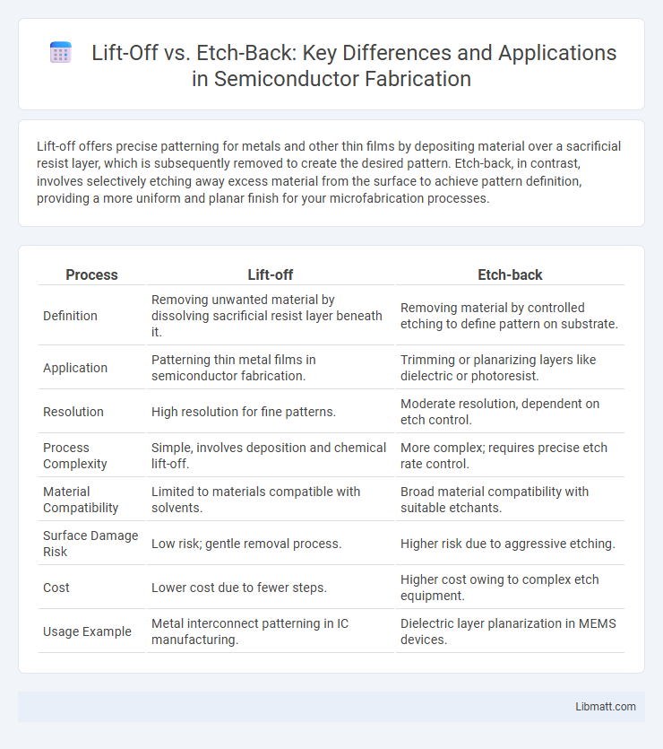
Table of Comparison
| Process | Lift-off | Etch-back |
|---|---|---|
| Definition | Removing unwanted material by dissolving sacrificial resist layer beneath it. | Removing material by controlled etching to define pattern on substrate. |
| Application | Patterning thin metal films in semiconductor fabrication. | Trimming or planarizing layers like dielectric or photoresist. |
| Resolution | High resolution for fine patterns. | Moderate resolution, dependent on etch control. |
| Process Complexity | Simple, involves deposition and chemical lift-off. | More complex; requires precise etch rate control. |
| Material Compatibility | Limited to materials compatible with solvents. | Broad material compatibility with suitable etchants. |
| Surface Damage Risk | Low risk; gentle removal process. | Higher risk due to aggressive etching. |
| Cost | Lower cost due to fewer steps. | Higher cost owing to complex etch equipment. |
| Usage Example | Metal interconnect patterning in IC manufacturing. | Dielectric layer planarization in MEMS devices. |
Introduction to Lift-off and Etch-back Techniques
Lift-off and etch-back techniques serve distinct purposes in microfabrication for defining precise patterns on substrates. Lift-off involves depositing a material over a patterned resist, which is then dissolved to remove excess material, ideal for metals and delicate structures. Etch-back uses controlled etching to remove layers selectively, suitable for planarizing surfaces and creating uniform thickness in thin films.
Definition and Overview of Lift-off Process
The lift-off process is a microfabrication technique used to create precise metal patterns on substrates by depositing material over a patterned resist and subsequent removal of the resist to lift off unwanted metal. This method contrasts with etch-back, where a blanket metal layer is deposited and selectively etched away to form patterns. Lift-off is preferred for its ability to produce high-resolution features with minimal damage to underlying layers, especially in complex circuit fabrication.
Definition and Overview of Etch-back Process
The etch-back process is a semiconductor fabrication technique used to planarize thin films by selectively removing excess material through controlled etching, creating uniform surface topography. This method contrasts with lift-off, which involves patterning via deposited material removal using a sacrificial resist layer. Etch-back offers precise depth control and is favored for applications requiring smooth surfaces and fine feature definition in integrated circuits.
Key Differences Between Lift-off and Etch-back
Lift-off and etch-back are distinct semiconductor fabrication techniques used for patterning thin films, where lift-off involves depositing a material over a patterned resist and removing the resist to leave the desired pattern, while etch-back removes excess material by etching down to a reference layer. Lift-off is ideal for metals and materials sensitive to etching, offering clean edges and minimal damage, whereas etch-back provides better planarity and thickness control by physically etching the unwanted areas. Your choice depends on the material properties and the required precision, with lift-off favoring delicate structures and etch-back suited for uniform surface finishes.
Applications of Lift-off in Microfabrication
Lift-off is widely applied in microfabrication for patterning thin films, especially in creating metal interconnects and electrodes in semiconductor devices. You benefit from its ability to precisely define complex geometries on photoresist layers without subjecting the substrate to harsh etching processes. This technique is essential for fabricating MEMS devices, LEDs, and integrated circuits where high-resolution patterning and material integrity are critical.
Applications of Etch-back in Semiconductor Manufacturing
Etch-back is widely applied in semiconductor manufacturing to achieve precise planarization and dimension control of thin films, particularly in processes like metal damascene and shallow trench isolation. This technique enhances device performance by creating uniform surface profiles essential for advanced integrated circuit fabrication. Your production yield and device reliability greatly benefit from etch-back's ability to remove excess materials without damaging underlying layers.
Advantages and Disadvantages of Lift-off
Lift-off offers precise patterning for thin metal films with simplicity and cost-effectiveness, making it ideal for delicate substrates and rapid prototyping. However, it struggles with thick metal layers due to poor edge definition and may lead to incomplete lift-off, causing defects. Etch-back provides cleaner edges and better thickness control but involves more complex processing and potential substrate damage.
Advantages and Disadvantages of Etch-back
Etch-back offers precise planarization by removing excess material, enhancing surface uniformity for improved device performance. It reduces potential defects caused by lift-off residues and allows better control over feature dimensions but requires more complex equipment and longer processing times. Your choice to use etch-back should consider its higher cost and process intricacy balanced against superior surface quality for advanced semiconductor manufacturing.
Selection Criteria: When to Use Lift-off vs Etch-back
Lift-off is ideal for patterning thin films with delicate or temperature-sensitive substrates where precise edge definition is crucial and deposition materials are difficult to etch. Etch-back suits applications requiring uniform film thickness and planar surfaces, especially for conductive interconnects or when high aspect ratio patterns are needed. Selection depends on factors like material compatibility, pattern resolution, substrate sensitivity, and process complexity, with lift-off favored for complex metal patterns and etch-back preferred for thicker dielectric layers or when anisotropic etching is achievable.
Future Trends in Patterning Technologies
Future trends in patterning technologies emphasize the integration of lift-off and etch-back techniques to enhance nanoscale precision and scalability in semiconductor manufacturing. Advances in lift-off materials and etch-back processes enable higher resolution patterning, reduced defects, and improved compatibility with emerging 3D architectures. Your ability to leverage these innovations will drive breakthroughs in device performance and miniaturization across next-generation electronics.
Lift-off vs Etch-back Infographic