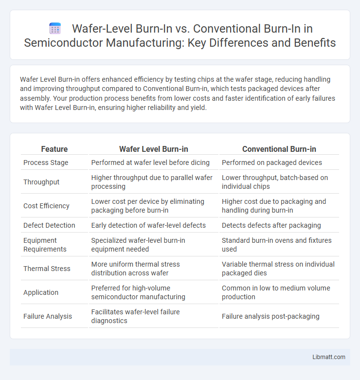
Wafer Level Burn-in offers enhanced efficiency by testing chips at the wafer stage, reducing handling and improving throughput compared to Conventional Burn-in, which tests packaged devices after assembly. Your production process benefits from lower costs and faster identification of early failures with Wafer Level Burn-in, ensuring higher reliability and yield.
Table of Comparison
| Feature | Wafer Level Burn-in | Conventional Burn-in |
|---|---|---|
| Process Stage | Performed at wafer level before dicing | Performed on packaged devices |
| Throughput | Higher throughput due to parallel wafer processing | Lower throughput, batch-based on individual chips |
| Cost Efficiency | Lower cost per device by eliminating packaging before burn-in | Higher cost due to packaging and handling during burn-in |
| Defect Detection | Early detection of wafer-level defects | Detects defects after packaging |
| Equipment Requirements | Specialized wafer-level burn-in equipment needed | Standard burn-in ovens and fixtures used |
| Thermal Stress | More uniform thermal stress distribution across wafer | Variable thermal stress on individual packaged dies |
| Application | Preferred for high-volume semiconductor manufacturing | Common in low to medium volume production |
| Failure Analysis | Facilitates wafer-level failure diagnostics | Failure analysis post-packaging |
Introduction to Burn-in Testing in Semiconductor Manufacturing
Burn-in testing in semiconductor manufacturing ensures device reliability by exposing integrated circuits to elevated stress conditions to identify early-life failures. Wafer Level Burn-in (WLB) applies this process directly to wafers before dicing, enhancing throughput and reducing handling risks compared to Conventional Burn-in, which tests individual packaged chips. Your selection between WLB and Conventional Burn-in can influence yield optimization, cost efficiency, and overall product quality in semiconductor production.
Defining Wafer Level Burn-in: Processes and Purpose
Wafer Level Burn-in involves subjecting entire semiconductor wafers to stress tests such as elevated temperature and voltage to detect early-life failures before dicing. This process improves reliability by identifying weak die units at the wafer stage, reducing costs associated with packaging and assembly of defective chips. Your production yields benefit from Wafer Level Burn-in by ensuring only robust devices proceed to subsequent manufacturing steps.
Understanding Conventional Burn-in Methods
Conventional burn-in involves subjecting packaged semiconductor devices to elevated temperature and voltage stresses to identify early-life failures, ensuring reliability before shipment. This process is typically performed at the final package level, increasing thermal resistance and limiting stress uniformity compared to wafer-level procedures. As a standard in the industry, conventional burn-in remains essential for legacy devices lacking wafer-level test capabilities, despite higher costs and longer cycle times.
Key Differences Between Wafer Level and Conventional Burn-in
Wafer Level Burn-in involves testing semiconductor wafers before dicing, allowing simultaneous stress application to all devices on the wafer, which enhances throughput and reduces packaging costs. Conventional Burn-in tests individual packaged devices, resulting in longer processing times and higher labor expenses due to separate handling. The wafer-level approach achieves better thermal uniformity and early detection of wafer defects, improving overall device reliability compared to post-packaging Conventional Burn-in.
Advantages of Wafer Level Burn-in
Wafer Level Burn-in offers significant advantages over Conventional Burn-in, including improved throughput due to parallel processing of multiple chips on the wafer, which reduces overall testing time and cost. This method enhances reliability by detecting early-life failures at the wafer stage, preventing defective dies from proceeding to packaging and assembly. Furthermore, Wafer Level Burn-in enables better thermal and electrical uniformity, leading to more consistent stress conditions and higher yield in semiconductor manufacturing.
Limitations and Challenges of Wafer Level Burn-in
Wafer Level Burn-in faces limitations such as high equipment costs and difficulties in maintaining uniform temperature and stress across the entire wafer, which can impact test accuracy. The challenge of effectively detecting latent defects at the wafer level arises due to complex thermal management and potential wafer warpage. Your reliability assurance may be constrained by these factors, making wafer-level burn-in less suitable for certain high-stress applications compared to conventional burn-in methods.
Benefits of Conventional Burn-in Approaches
Conventional burn-in approaches provide proven reliability by effectively identifying early-life failures in semiconductor devices through individual chip testing under elevated stress conditions. This method ensures thorough screening for defect-induced failures and helps improve long-term product quality by eliminating weak components before packaging. Despite higher costs and time requirements compared to Wafer Level Burn-in, conventional burn-in remains a trusted process for critical applications requiring robust performance validation.
Cost and Efficiency Comparison: Wafer Level vs. Conventional Burn-in
Wafer Level Burn-in reduces overall costs by enabling simultaneous testing of multiple chips directly on the wafer, minimizing handling and packaging expenses compared to Conventional Burn-in, which requires individual chip testing after packaging. Efficiency is significantly improved in Wafer Level Burn-in due to faster thermal cycling and higher throughput, allowing earlier defect identification and reduced time-to-market. Your manufacturing process benefits from lower operational costs and better resource utilization with Wafer Level Burn-in technology.
Applications and Industry Adoption Trends
Wafer Level Burn-in (WLB) is increasingly utilized in advanced semiconductor applications such as high-performance computing, automotive electronics, and 5G devices due to its ability to screen defects earlier in the manufacturing process, reducing overall production costs and improving yield. Conventional Burn-in remains prevalent in mature industries like consumer electronics and memory chips where process maturity and cost efficiency are prioritized, but it is gradually being supplemented by WLB for advanced node technologies. Industry adoption trends highlight a shift towards Wafer Level Burn-in driven by the demand for higher reliability, shorter time-to-market, and integration with wafer-level testing methodologies in logic and mixed-signal IC manufacturing.
Future Outlook: Evolving Burn-in Technologies in Semiconductor Testing
Future outlook in semiconductor testing highlights Wafer Level Burn-in (WLB) as a transformative technology that enhances efficiency by enabling simultaneous stress testing of entire wafers, reducing time and cost compared to Conventional Burn-in. Advances in WLB are expected to further improve thermal management and defect detection accuracy, supporting the demands of increasingly complex integrated circuits. Your semiconductor manufacturing process can benefit from WLB's scalability and integration with automation, positioning it as a key driver for next-generation device reliability.
Wafer Level Burn-in vs Conventional Burn-in Infographic