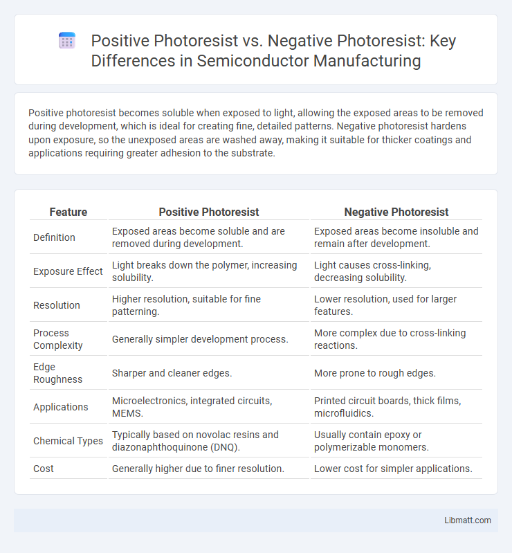
Positive photoresist becomes soluble when exposed to light, allowing the exposed areas to be removed during development, which is ideal for creating fine, detailed patterns. Negative photoresist hardens upon exposure, so the unexposed areas are washed away, making it suitable for thicker coatings and applications requiring greater adhesion to the substrate.
Table of Comparison
| Feature | Positive Photoresist | Negative Photoresist |
|---|---|---|
| Definition | Exposed areas become soluble and are removed during development. | Exposed areas become insoluble and remain after development. |
| Exposure Effect | Light breaks down the polymer, increasing solubility. | Light causes cross-linking, decreasing solubility. |
| Resolution | Higher resolution, suitable for fine patterning. | Lower resolution, used for larger features. |
| Process Complexity | Generally simpler development process. | More complex due to cross-linking reactions. |
| Edge Roughness | Sharper and cleaner edges. | More prone to rough edges. |
| Applications | Microelectronics, integrated circuits, MEMS. | Printed circuit boards, thick films, microfluidics. |
| Chemical Types | Typically based on novolac resins and diazonaphthoquinone (DNQ). | Usually contain epoxy or polymerizable monomers. |
| Cost | Generally higher due to finer resolution. | Lower cost for simpler applications. |
Introduction to Photoresists
Photoresists are light-sensitive materials crucial for microfabrication processes, categorized mainly into positive and negative types based on their reaction to exposure. Positive photoresists become more soluble when exposed to light, allowing the exposed pattern to be removed during development, while negative photoresists harden and become insoluble, preserving the exposed areas. These materials are essential in semiconductor manufacturing, printed circuit board production, and nanotechnology for creating precise micro- and nanoscale patterns.
What is Positive Photoresist?
Positive photoresist is a light-sensitive material used in photolithography where the exposed areas become more soluble in a developer solution, allowing selective removal to create a patterned layer. This characteristic enables precise transfer of circuit designs onto semiconductor wafers, essential for microfabrication in electronics. Your choice of positive photoresist ensures high-resolution patterning crucial for advanced semiconductor manufacturing processes.
What is Negative Photoresist?
Negative photoresist is a type of photosensitive material that becomes insoluble when exposed to ultraviolet (UV) light, allowing the exposed regions to remain on the substrate after development. It is commonly used in photolithography for patterning microelectronic circuits and MEMS devices due to its high chemical resistance and strong adhesion. Negative photoresist typically offers better etch resistance and thicker film applications compared to positive photoresist, making it ideal for certain manufacturing processes.
Key Differences Between Positive and Negative Photoresists
Positive photoresists become soluble when exposed to light, allowing the exposed regions to be washed away during development, while negative photoresists harden upon exposure, causing the unexposed areas to be removed. You should choose positive photoresists for high-resolution patterning due to their fine detail capabilities, whereas negative photoresists offer better adhesion and durability for thicker coatings. Understanding these key differences is crucial for selecting the appropriate photoresist in semiconductor lithography and microfabrication processes.
Working Principles of Positive Photoresist
Positive photoresist functions by becoming soluble in a developer solution upon exposure to ultraviolet (UV) light, allowing selective removal of the exposed regions during the development phase. This photochemical reaction breaks down the polymer chains in the resist, enabling precise pattern formation on semiconductor wafers. The process facilitates high-resolution patterning essential for advanced lithography in microfabrication.
Working Principles of Negative Photoresist
Negative photoresist works by polymerizing exposed areas when subjected to ultraviolet (UV) light, making those regions insoluble in the developer solution. During the development process, the unexposed regions dissolve, leaving behind a patterned resist that protects parts of the substrate. This property enables the fabrication of precise microstructures in semiconductor and microelectromechanical systems (MEMS) applications.
Advantages of Positive Photoresists
Positive photoresists offer superior resolution and greater accuracy in pattern transfer, essential for advanced semiconductor fabrication. Their ability to produce finer features results from the selective exposure process where the exposed regions become soluble, enabling precise etching. This makes positive photoresists ideal for applications requiring high precision and detailed microfabrication.
Advantages of Negative Photoresists
Negative photoresists offer superior chemical resistance and better adhesion to substrates, making them ideal for applications requiring robust pattern durability. Their ability to create finer, high-aspect-ratio features enhances precision in microfabrication processes. You benefit from lower exposure doses and simplified processing steps, which reduce manufacturing time and costs.
Applications: When to Choose Positive or Negative Photoresist
Positive photoresists are ideal for applications requiring high-resolution patterning, such as semiconductor device fabrication and fine-feature microelectronics, because they become soluble in exposed areas, enabling precise etching of complex circuits. Negative photoresists are preferred for applications involving thick films and robust structures like MEMS, printed circuit boards, and optical devices, since they polymerize upon exposure, producing durable patterns suitable for harsh processing conditions. The choice depends on the desired resolution, pattern complexity, and the chemical or mechanical robustness required for the final microfabrication process.
Conclusion: Selecting the Right Photoresist for Your Process
Choosing the right photoresist hinges on the specific requirements of your lithography process, including resolution, pattern complexity, and substrate compatibility. Positive photoresists offer high resolution and ease of patterning, making them ideal for fine-feature semiconductor fabrication. Negative photoresists provide better adhesion and chemical resistance, suitable for thicker coatings and MEMS applications.
Positive Photoresist vs Negative Photoresist Infographic