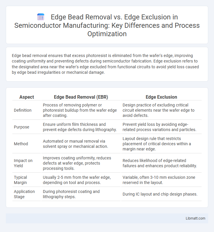
Edge bead removal ensures that excess photoresist is eliminated from the wafer's edge, improving coating uniformity and preventing defects during semiconductor fabrication. Edge exclusion refers to the designated area near the wafer's edge excluded from functional circuits to avoid yield loss caused by edge bead irregularities or mechanical damage.
Table of Comparison
| Aspect | Edge Bead Removal (EBR) | Edge Exclusion |
|---|---|---|
| Definition | Process of removing polymer or photoresist buildup from the wafer edge after coating. | Design practice of excluding critical circuit elements near the wafer edge to avoid defects. |
| Purpose | Ensure uniform film thickness and prevent edge defects during lithography. | Prevent yield loss by avoiding edge-related process variations and particles. |
| Method | Automated or manual removal via solvent spray or mechanical action. | Layout design rule that restricts placement of critical devices within a margin near edge. |
| Impact on Yield | Improves coating uniformity, reduces defects at wafer edge, protects processing tools. | Reduces likelihood of edge-related failures and enhances product reliability. |
| Typical Margin | Usually 2-5 mm from the wafer edge, depending on tool and process. | Variable, often 3-10 mm exclusion zone reserved in the layout. |
| Application Stage | During photoresist coating and lithography steps. | During IC layout and chip design phases. |
Introduction to Edge Bead Removal and Edge Exclusion
Edge Bead Removal (EBR) and Edge Exclusion are critical processes in semiconductor photolithography to improve pattern accuracy and yield. Edge Bead Removal involves eliminating excess photoresist from the wafer edge to prevent defects during exposure and development, while Edge Exclusion defines a non-patterned margin near the wafer edge where no circuitry is fabricated to avoid process inconsistencies. These techniques optimize lithographic quality by minimizing edge-related defects and ensuring uniform film thickness across the wafer surface.
Defining Edge Bead Removal
Edge Bead Removal refers to the precise process of eliminating excess photoresist material from the periphery of a semiconductor wafer edge to ensure uniform coating thickness and prevent defects during lithography. This technique improves pattern fidelity by avoiding resist buildup that can cause mask misalignment and printing errors. Proper edge bead removal is essential for optimizing wafer surface quality and enhancing yield in microfabrication processes.
Understanding Edge Exclusion
Edge exclusion refers to the deliberate avoidance of measuring or analyzing regions near the wafer's edge during semiconductor inspection to prevent inaccurate data caused by process variations and edge bead effects. Unlike edge bead removal, which physically strips excess photoresist to create a uniform edge, edge exclusion sets a predefined boundary inside the wafer perimeter where metrology systems ignore data. This technique improves yield analysis by focusing on the stable central regions, reducing false defect counts and enhancing process control.
Key Differences Between Edge Bead Removal and Edge Exclusion
Edge Bead Removal (EBR) eliminates excess photoresist buildup along wafer edges during semiconductor fabrication, ensuring uniform coating and preventing defects in lithography. Edge Exclusion defines a no-process zone at the wafer periphery where patterning or processing steps are intentionally avoided to enhance yield and avoid edge-related defects. The key difference lies in EBR physically removing unwanted resist material, while Edge Exclusion restricts patterning area without altering the resist layer itself.
Importance in Semiconductor Manufacturing
Edge bead removal ensures uniform photoresist coating by eliminating excess material from wafer edges, which prevents defects during lithography and improves yield in semiconductor manufacturing. Edge exclusion designates a non-patterned margin near the wafer edge to avoid process variations and contamination, thereby maintaining device reliability and performance. Proper management of both techniques is critical for Your semiconductor fabrication process to achieve high-quality, defect-free integrated circuits.
Process Flow: Edge Bead Removal Techniques
Edge bead removal techniques involve the precise elimination of excess photoresist at the wafer's perimeter to prevent defects during lithography. Common methods include mechanical scraping, plasma etching, and solvent-based processes that ensure uniform coating and improve pattern fidelity. These techniques maintain process consistency by avoiding edge exclusion zones, maximizing usable wafer area for device fabrication.
Edge Exclusion Methods and Applications
Edge exclusion methods involve intentionally ignoring the outer regions of a semiconductor wafer during photolithography to prevent defects caused by uneven resist coating or exposure. These techniques are critical in applications such as IC manufacturing where precise pattern fidelity near wafer edges is essential for high device yield. Common edge exclusion methods include mechanical masking and controlled resist application, both ensuring that the peripheral areas do not interfere with the functional circuit patterns.
Impact on Yield and Wafer Quality
Edge bead removal (EBR) enhances wafer yield by preventing photoresist accumulation at the wafer edges, reducing defects during lithography and ensuring uniform coating. Edge exclusion limits the usable wafer area to avoid edge defects, which decreases potential yield but improves overall wafer quality by eliminating high-risk zones. Optimizing EBR processes can maximize active device area without sacrificing wafer integrity, balancing yield improvement with quality control.
Industry Standards and Best Practices
Edge Bead Removal (EBR) and Edge Exclusion are critical processes in PCB manufacturing, ensuring solder mask adhesion and preventing defective solder joints. Industry standards such as IPC-6012 mandate strict control over edge bead thickness and uniformity, highlighting Edge Bead Removal to maintain optimal PCB surface quality. Your manufacturing process should integrate precise Edge Bead Removal techniques alongside controlled Edge Exclusion zones to comply with best practices and achieve high reliability in electronic assemblies.
Future Trends in Edge Processing Technologies
Future trends in edge processing technologies emphasize increased automation and precision in edge bead removal, leveraging AI-driven inspection systems to minimize defects on printed circuit boards. Advances in machine learning algorithms enable real-time adjustments during edge exclusion processes, enhancing yield and reducing material waste. Integration of IoT and smart sensors is poised to optimize edge processing workflows, driving efficiency in semiconductor manufacturing and flexible electronics production.
Edge Bead Removal vs Edge Exclusion Infographic