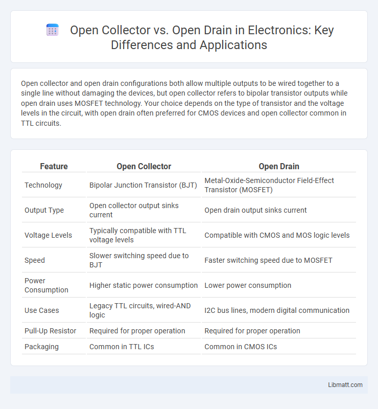
Open collector and open drain configurations both allow multiple outputs to be wired together to a single line without damaging the devices, but open collector refers to bipolar transistor outputs while open drain uses MOSFET technology. Your choice depends on the type of transistor and the voltage levels in the circuit, with open drain often preferred for CMOS devices and open collector common in TTL circuits.
Table of Comparison
| Feature | Open Collector | Open Drain |
|---|---|---|
| Technology | Bipolar Junction Transistor (BJT) | Metal-Oxide-Semiconductor Field-Effect Transistor (MOSFET) |
| Output Type | Open collector output sinks current | Open drain output sinks current |
| Voltage Levels | Typically compatible with TTL voltage levels | Compatible with CMOS and MOS logic levels |
| Speed | Slower switching speed due to BJT | Faster switching speed due to MOSFET |
| Power Consumption | Higher static power consumption | Lower power consumption |
| Use Cases | Legacy TTL circuits, wired-AND logic | I2C bus lines, modern digital communication |
| Pull-Up Resistor | Required for proper operation | Required for proper operation |
| Packaging | Common in TTL ICs | Common in CMOS ICs |
Introduction to Open Collector and Open Drain
Open Collector and Open Drain are types of transistor output configurations commonly used in digital circuits for interfacing and signal control. Open Collector typically refers to a bipolar junction transistor output where the collector is left "open" for external pull-up resistors, while Open Drain is its MOSFET equivalent with the drain terminal left open. Your choice between Open Collector and Open Drain depends on the specific device technology and the voltage levels required in your electronic designs.
Basic Working Principle
Open Collector and Open Drain outputs both operate by using a transistor to pull the output line to ground when active, allowing external components to define the high state. Open Collector refers to bipolar junction transistor (BJT) configurations, where the collector is exposed as the output node. Open Drain uses a MOSFET transistor with the drain connected to the output, functioning similarly but optimized for CMOS technology and offering faster switching speeds.
Technical Differences Explained
Open collector outputs are typically found in bipolar junction transistor (BJT) circuits, using the transistor's collector terminal as the output stage, allowing sinking current but requiring an external pull-up resistor for voltage high state. Open drain outputs use MOSFET transistors, connecting the drain terminal to the output, similarly needing a pull-up resistor to reach a high level, but they offer faster switching speeds and lower on-resistance compared to open collector. Both configurations support wired-AND logic and level shifting, but open drain is preferred in modern low-voltage, high-speed digital interfaces such as I2C and GPIO pins.
Common Use Cases
Open Collector outputs are commonly used in transistor-transistor logic (TTL) circuits for wired-AND configurations and level shifting, while Open Drain outputs are prevalent in MOSFET-based systems like I2C communication buses for their effective multi-device bus communication capabilities. Your choice between the two depends on the type of semiconductor technology and voltage levels required in the application. Both configurations enable multiple outputs to safely share a single line without electrical conflict, facilitating signal interfacing and bus arbitration.
Voltage Compatibility and Level Shifting
Open Collector outputs are typically used with bipolar junction transistors (BJTs) and operate within the voltage range supported by the transistor's collector, while Open Drain outputs use MOSFETs that tolerate higher voltages and faster switching speeds. Voltage compatibility depends on the pull-up resistor voltage level, making level shifting easier in Open Drain configurations due to their MOSFET structure, which supports a wider voltage range without damage. Your choice between Open Collector and Open Drain impacts how you implement level shifting and ensure reliable interfacing between differing voltage domains in mixed-technology circuits.
Circuit Design Considerations
Open collector and open drain circuits both enable multiple devices to share a communication line by using a transistor to pull the line low, requiring an external pull-up resistor to restore the line to a high state. Open collector utilizes bipolar junction transistors (BJTs), while open drain uses metal-oxide-semiconductor field-effect transistors (MOSFETs), affecting switching speed and voltage levels in circuit design. Designers must consider transistor type, pull-up resistor values, voltage compatibility, and signal integrity when choosing between open collector and open drain configurations for bus systems or digital logic interfacing.
Pull-up Resistors: Importance and Selection
Pull-up resistors are critical in both open collector and open drain configurations to define the default high logic level when the transistor is not pulling the line low. The resistor value selection balances power consumption and switching speed, with typical values ranging from 4.7kO to 10kO depending on bus capacitance and desired rise time. Correct pull-up resistor sizing ensures reliable signal integrity by preventing floating lines and minimizing noise susceptibility in digital circuits.
Advantages of Open Collector and Open Drain
Open Collector and Open Drain configurations offer significant advantages in digital circuit design by allowing multiple outputs to share a single line for wired-AND or wired-OR logic functions, simplifying signal interfacing and expanding system flexibility. Open Collector outputs, typically used with bipolar transistors, provide robust switching capabilities and are ideal for driving loads at varying voltage levels, while Open Drain outputs, using MOSFET transistors, consume lower power and produce less heat, enhancing energy efficiency in integrated circuits. Both types enable easy level shifting and fault tolerance, making them essential for communication protocols like I2C and multi-device bus systems.
Limitations and Potential Issues
Open Collector outputs are limited by the external pull-up resistor, which affects the speed and voltage levels, potentially causing slower rise times and increased power dissipation. Open Drain configurations face challenges with voltage compatibility and require careful selection of pull-up voltages to avoid damage or malfunction. Your circuit design must address these limitations to ensure reliable signal integrity and proper interfacing with other components.
Application Examples in Modern Electronics
Open collector outputs are commonly used in transistor-transistor logic (TTL) circuits for wired-AND connections and level shifting between different voltage domains. Open drain configurations dominate in modern electronics like I2C communication buses and MOSFET-based switching circuits due to their compatibility with various voltage levels and low power consumption. Understanding these applications helps you design efficient interfaces and communication protocols in embedded systems.
Open Collector vs Open Drain Infographic