NPN transistors conduct when a positive voltage is applied to the base, allowing current to flow from collector to emitter, making them ideal for switching and amplification in common ground circuits. PNP transistors conduct when the base is pulled to a lower voltage than the emitter, enabling current flow from emitter to collector, which suits applications requiring a positive supply voltage.
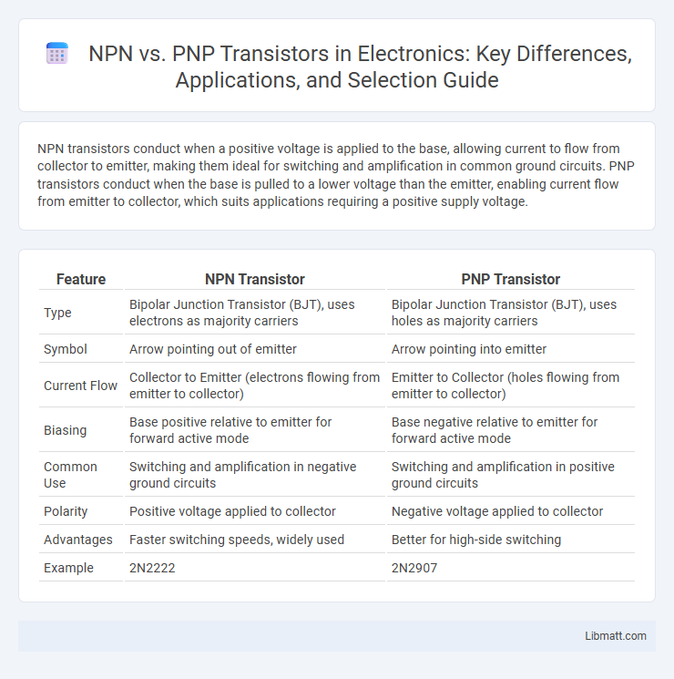
Table of Comparison
| Feature | NPN Transistor | PNP Transistor |
|---|---|---|
| Type | Bipolar Junction Transistor (BJT), uses electrons as majority carriers | Bipolar Junction Transistor (BJT), uses holes as majority carriers |
| Symbol | Arrow pointing out of emitter | Arrow pointing into emitter |
| Current Flow | Collector to Emitter (electrons flowing from emitter to collector) | Emitter to Collector (holes flowing from emitter to collector) |
| Biasing | Base positive relative to emitter for forward active mode | Base negative relative to emitter for forward active mode |
| Common Use | Switching and amplification in negative ground circuits | Switching and amplification in positive ground circuits |
| Polarity | Positive voltage applied to collector | Negative voltage applied to collector |
| Advantages | Faster switching speeds, widely used | Better for high-side switching |
| Example | 2N2222 | 2N2907 |
Introduction to NPN and PNP Transistors
NPN and PNP transistors are fundamental components in electronic circuits, distinguished by their internal structure and current flow directions. NPN transistors consist of a layer of P-type semiconductor sandwiched between two N-type layers, allowing electrons to flow from the emitter to the collector when a positive voltage is applied to the base. PNP transistors have the opposite configuration, with a layer of N-type material between two P-type layers, enabling current flow from emitter to collector when a negative voltage is applied to the base, affecting how your circuit is designed and controlled.
Understanding the Basic Structure
NPN and PNP transistors differ fundamentally in their semiconductor layers; an NPN transistor consists of a layer of P-type semiconductor sandwiched between two N-type layers, while a PNP transistor has an N-type layer between two P-type layers. This arrangement affects the direction of current flow and the type of charge carriers involved--electrons for NPN and holes for PNP transistors. Understanding this basic structure helps you select the appropriate transistor type for switching or amplification tasks in electronic circuits.
Key Differences Between NPN and PNP
NPN transistors have electrons as the majority charge carriers, whereas PNP transistors use holes. In an NPN transistor, current flows from the collector to the emitter when a positive voltage is applied to the base, while in a PNP transistor, current flows from the emitter to the collector with a negative base voltage. Your choice between NPN and PNP depends on the specific circuit design and voltage requirements.
Symbol Representations in Circuit Diagrams
NPN and PNP transistors are distinguished by their symbol representations in circuit diagrams, where the arrow on the emitter terminal indicates current flow direction. In an NPN transistor symbol, the arrow points outward, signifying current flows from the emitter to the base, while in a PNP transistor, the arrow points inward, showing current flow from the base to the emitter. Understanding these symbol differences is crucial for correctly interpreting and designing your electronic circuits.
How NPN Transistors Work
NPN transistors operate by allowing current flow from the collector to the emitter when a small current is applied to the base, triggering electron movement from the emitter, through the base, to the collector. The base-emitter junction is forward-biased, enabling electron injection from the n-type emitter into the p-type base, while the base-collector junction is reverse-biased to facilitate electron collection. This controlled electron flow amplifies current and switches circuits efficiently, distinguishing NPN transistors from PNP types that rely on hole movement and opposite polarity.
How PNP Transistors Work
PNP transistors operate by allowing current flow from the emitter to the collector when a small current is applied to the base terminal, with the emitter being more positive relative to the base. The majority carriers, holes, move from the emitter to the base region, enabling current conduction through the transistor. This behavior contrasts with NPN transistors, where electrons serve as the majority carriers, highlighting the importance of polarity in transistor operation.
Common Applications of NPN Transistors
NPN transistors are widely used in switching applications and amplification circuits due to their fast-switching capabilities and ease of control in positive voltage environments. They are commonly found in digital logic circuits, motor drivers, and LED drivers, where the emitter is connected to ground and the collector to the load. Their prevalence in low-side switching makes them the preferred choice in most electronic devices requiring efficient current control.
Common Applications of PNP Transistors
PNP transistors are commonly used in low-side switch configurations, where the transistor connects the load to ground, enabling control of devices such as relays, LEDs, and motors. They are also preferred in positive voltage sensing and current sourcing applications, particularly in automotive and industrial control systems. PNP transistors efficiently manage current flow from the emitter to the collector, making them suitable for circuits requiring voltage regulation and amplification in the negative voltage domain.
Choosing Between NPN and PNP for Your Project
Choosing between NPN and PNP transistors depends on the specific requirements of your project, including the type of load and power supply configuration. NPN transistors are generally preferred for switching applications where the ground is common, offering faster operation and easier interfacing with microcontrollers. PNP transistors are better suited for high-side switching and positive voltage control, providing efficient current sourcing in circuits where the positive voltage rail is common.
Summary: NPN vs PNP at a Glance
NPN transistors consist of a layer of P-type semiconductor between two N-type layers, allowing electrons to flow from the emitter to the collector, making them suitable for switching and amplification in positive voltage circuits. PNP transistors have a layer of N-type semiconductor between two P-type layers, with holes as the majority carriers, enabling current flow from the emitter to the collector in negative voltage or ground-referenced circuits. Your choice between NPN and PNP depends on the circuit polarity and current direction requirements for optimal performance.
NPN vs PNP Infographic