N-type semiconductors contain extra electrons as majority carriers due to donor impurities, enhancing electrical conductivity, while P-type semiconductors have holes as majority carriers created by acceptor impurities. Understanding these differences is essential for designing and optimizing your electronic devices for specific functions.
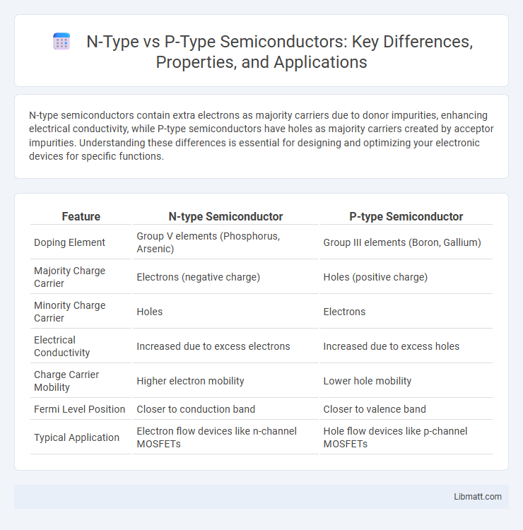
Table of Comparison
| Feature | N-type Semiconductor | P-type Semiconductor |
|---|---|---|
| Doping Element | Group V elements (Phosphorus, Arsenic) | Group III elements (Boron, Gallium) |
| Majority Charge Carrier | Electrons (negative charge) | Holes (positive charge) |
| Minority Charge Carrier | Holes | Electrons |
| Electrical Conductivity | Increased due to excess electrons | Increased due to excess holes |
| Charge Carrier Mobility | Higher electron mobility | Lower hole mobility |
| Fermi Level Position | Closer to conduction band | Closer to valence band |
| Typical Application | Electron flow devices like n-channel MOSFETs | Hole flow devices like p-channel MOSFETs |
Understanding N-type and P-type Semiconductors
N-type semiconductors are created by doping a pure semiconductor with elements that have more valence electrons, typically adding phosphorus or arsenic, which contribute free electrons as charge carriers. P-type semiconductors result from doping with elements like boron or gallium that have fewer valence electrons, creating "holes" or positive charge carriers within the material. Understanding the difference between N-type and P-type semiconductors is essential for designing your electronic devices, as these complementary materials form the basis of diodes, transistors, and integrated circuits.
Key Differences Between N-type and P-type
N-type semiconductors contain excess electrons as the majority carriers, introduced by doping with elements like phosphorus, which donate extra electrons. P-type semiconductors feature holes as majority carriers, created by doping with elements such as boron that accept electrons, resulting in positive charge carriers. Your choice between N-type and P-type materials depends on the desired electrical properties for devices like diodes, transistors, or integrated circuits.
How N-type Semiconductors Work
N-type semiconductors work by adding impurities, such as phosphorus or arsenic, to intrinsic silicon, introducing extra electrons that increase conductivity. These free electrons serve as the majority charge carriers, allowing electric current to flow efficiently through the material. Understanding how N-type semiconductors function helps you optimize electronic devices like diodes and transistors for faster performance.
Mechanism of P-type Semiconductors
P-type semiconductors are created by doping intrinsic silicon with elements like boron, which have one less valence electron than silicon, resulting in the formation of "holes" or positive charge carriers. These holes act as the majority charge carriers, allowing electric current to flow by the movement of electrons filling these vacancies. The presence of acceptor impurity atoms creates energy levels just above the valence band, facilitating hole conduction under an applied electric field.
Doping Materials for N-type and P-type
N-type semiconductors are doped with elements like phosphorus, arsenic, or antimony, which have five valence electrons, providing extra electrons to enhance conductivity. P-type semiconductors use doping materials such as boron, aluminum, or gallium, containing three valence electrons, creating "holes" or positive charge carriers. Your choice of doping material directly influences the electrical properties and behavior of the semiconductor device.
Electrical Conductivity Comparison
N-type semiconductors exhibit higher electrical conductivity compared to P-type materials due to the abundance of free electrons, which have greater mobility than holes in P-type semiconductors. The presence of donor atoms in N-type doping introduces extra electrons into the conduction band, enhancing charge carrier density and overall conductivity. Your choice between N-type and P-type will significantly impact the efficiency of electronic devices, especially in applications demanding optimal electrical performance.
Applications of N-type Semiconductors
N-type semiconductors are widely used in electronic devices requiring efficient electron conduction, such as transistors, diodes, and integrated circuits. Their enhanced electron mobility makes them ideal for high-speed and high-frequency applications in modern electronics. Your choice of N-type materials can significantly improve the performance of sensors, solar cells, and various semiconductor devices.
Applications of P-type Semiconductors
P-type semiconductors are widely used in photovoltaic cells, where they serve as the base layer for efficient light absorption and charge carrier generation. They are essential in creating p-n junctions in diodes and transistors, enabling controlled electrical conductivity for switching and amplification in electronic devices. These materials also find applications in thermoelectric devices, where their hole conductivity contributes to converting temperature differences into electrical voltage.
Role in Electronic Devices and Circuits
N-type semiconductors, enriched with electrons as majority carriers, provide high conductivity essential for electron flow in electronic devices and circuits. P-type semiconductors, containing holes as majority carriers, facilitate current by enabling hole movement, complementing N-type materials in junctions like diodes and transistors. The interaction between N-type and P-type regions forms the basis of critical components such as PN junctions, bipolar junction transistors (BJTs), and MOSFETs, enabling controlled switching and amplification in modern electronics.
Choosing Between N-type and P-type Semiconductors
Choosing between N-type and P-type semiconductors depends on your specific application requirements, including conductivity type and charge carrier behavior. N-type semiconductors, doped with elements like phosphorus, provide an excess of electrons for higher electron mobility, making them ideal for faster switching and low-resistance circuits. P-type semiconductors, doped with elements such as boron, create holes as the majority charge carriers, useful in creating p-n junctions crucial for diodes and transistor functions.
N-type vs P-type Infographic