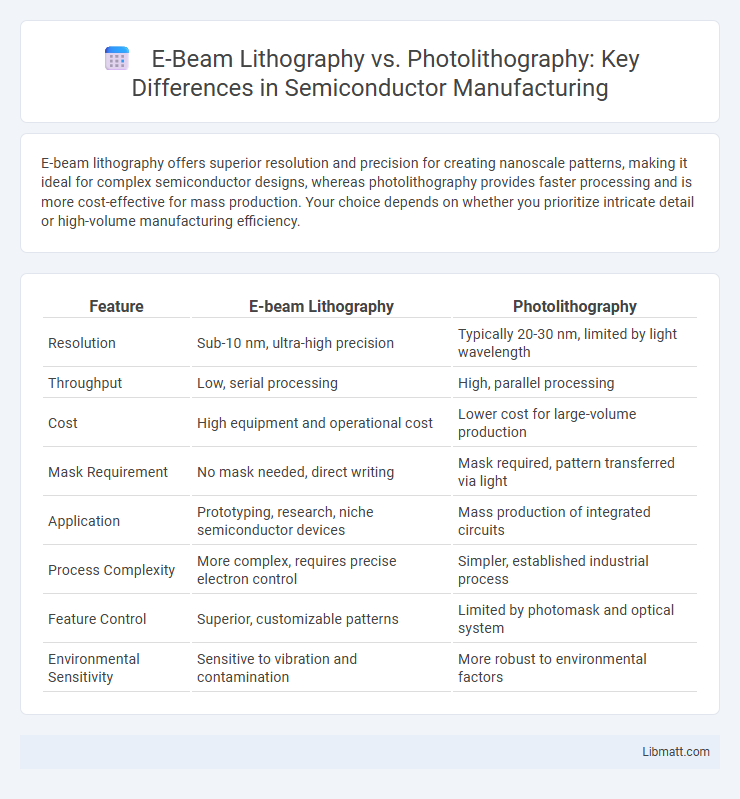
E-beam lithography offers superior resolution and precision for creating nanoscale patterns, making it ideal for complex semiconductor designs, whereas photolithography provides faster processing and is more cost-effective for mass production. Your choice depends on whether you prioritize intricate detail or high-volume manufacturing efficiency.
Table of Comparison
| Feature | E-beam Lithography | Photolithography |
|---|---|---|
| Resolution | Sub-10 nm, ultra-high precision | Typically 20-30 nm, limited by light wavelength |
| Throughput | Low, serial processing | High, parallel processing |
| Cost | High equipment and operational cost | Lower cost for large-volume production |
| Mask Requirement | No mask needed, direct writing | Mask required, pattern transferred via light |
| Application | Prototyping, research, niche semiconductor devices | Mass production of integrated circuits |
| Process Complexity | More complex, requires precise electron control | Simpler, established industrial process |
| Feature Control | Superior, customizable patterns | Limited by photomask and optical system |
| Environmental Sensitivity | Sensitive to vibration and contamination | More robust to environmental factors |
Introduction to E-beam Lithography and Photolithography
E-beam lithography utilizes a focused beam of electrons to write custom patterns with nanometer precision directly onto a resist-coated substrate, enabling high-resolution semiconductor fabrication and prototyping. Photolithography employs ultraviolet light projected through a photomask to transfer patterns onto a photoresist layer, offering high throughput and scalability for mass production in integrated circuit manufacturing. While e-beam lithography excels in flexibility and resolution, photolithography remains the industry standard for large-scale semiconductor fabrication due to its speed and cost efficiency.
Core Principles of E-beam Lithography
E-beam lithography uses a focused beam of electrons to directly write patterns onto a resist-coated substrate, enabling nanometer-scale resolution beyond the limits of photolithography. Unlike photolithography, which relies on masks and ultraviolet light, e-beam lithography offers maskless patterning, enhancing flexibility for prototype development and custom designs. Your precision in fabricating intricate semiconductor devices depends on e-beam lithography's ability to control electron exposure doses and beam deflection with extreme accuracy.
Fundamentals of Photolithography
Photolithography relies on ultraviolet light to transfer geometric patterns from a photomask onto a photosensitive resist coating a semiconductor wafer, enabling precise microfabrication of integrated circuits. The process involves exposure, development, and etching steps that define intricate circuit features with high throughput and scalability. Key factors influencing photolithography include wavelength of light, numerical aperture, and resist sensitivity, which determine resolution and accuracy in semiconductor manufacturing.
Resolution Capabilities: E-beam vs Photolithography
E-beam lithography offers superior resolution capabilities, enabling feature sizes below 10 nanometers due to its direct-write electron beam exposure, which surpasses the diffraction limits of photolithography. Photolithography typically achieves minimum feature sizes around 20-30 nanometers using advanced techniques like extreme ultraviolet (EUV) lithography but struggles to match the ultra-high precision of E-beam lithography. This resolution advantage makes E-beam lithography ideal for prototype development and nano-scale device fabrication, whereas photolithography remains the preferred method for high-throughput semiconductor manufacturing.
Throughput and Production Scalability
E-beam lithography offers high-resolution patterning ideal for prototyping and small-scale production but suffers from low throughput due to its serial writing process. Photolithography excels in production scalability with rapid parallel processing, enabling mass manufacturing of semiconductor devices at high volumes. The choice between the two hinges on balancing E-beam's precision against photolithography's efficiency for large-scale throughput.
Material Compatibility and Process Flexibility
E-beam lithography offers superior material compatibility by directly writing on a wide range of substrates without masks, enabling high-resolution patterning on unconventional and sensitive materials such as polymers and biomolecules. Photolithography, while faster and more cost-effective for large-scale production, primarily relies on photoresists compatible with specific wavelength ranges and substrate types, limiting its applicability to standard semiconductor materials. Process flexibility in e-beam lithography allows intricate pattern customization and rapid design iterations, whereas photolithography's reliance on masks restricts modifications and is less adaptable to frequent design changes.
Cost Analysis and Economic Considerations
E-beam lithography incurs significantly higher costs than photolithography due to its slower throughput and expensive equipment, making it less suited for high-volume manufacturing. Photolithography benefits from economies of scale, enabling lower per-unit costs, especially in semiconductor production for large batches. Your choice between these technologies should weigh initial capital investment against production volume requirements and precision needs.
Application Areas and Industry Use Cases
E-beam lithography excels in applications requiring ultra-high-resolution patterning, such as semiconductor prototype fabrication, advanced photomask production, and nanotechnology research. Photolithography dominates mass production in the semiconductor industry, especially for integrated circuits, MEMS, and flat-panel displays due to its high throughput and scalability. Your choice between these technologies depends on the precision requirements and production volume of your manufacturing process.
Challenges and Limitations of Each Technology
E-beam lithography faces challenges such as slow writing speeds and limited throughput, making it less suitable for large-scale semiconductor manufacturing, while photolithography struggles with resolution limits due to the wavelength of light used. E-beam's high precision is offset by its cost and complexity, whereas photolithography requires costly masks and faces difficulties in patterning extremely small features below 10 nanometers. Your choice depends on balancing these limitations against production volume and feature size requirements.
Future Trends and Innovations in Lithography
Future trends in lithography emphasize the advancement of Extreme Ultraviolet (EUV) lithography and the integration of machine learning algorithms to optimize pattern precision in photolithography processes. E-beam lithography innovations focus on multi-beam technology and accelerated writing speeds to overcome throughput limitations, enabling high-resolution patterning for next-generation semiconductor devices. Hybrid approaches combining E-beam's nanoscale accuracy with photolithography's scalability are emerging to support the production of advanced integrated circuits and nanostructures.
E-beam Lithography vs Photolithography Infographic