Bulk silicon wafers offer a cost-effective substrate with excellent thermal conductivity and mechanical strength, making them ideal for general semiconductor applications. Your choice shifts to SOI (Silicon on Insulator) wafers when enhanced device performance, reduced parasitic capacitance, and improved isolation are critical, especially in high-speed and low-power electronics.
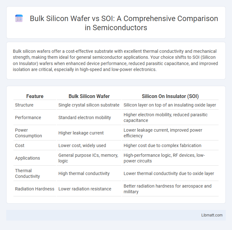
Table of Comparison
| Feature | Bulk Silicon Wafer | Silicon On Insulator (SOI) |
|---|---|---|
| Structure | Single crystal silicon substrate | Silicon layer on top of an insulating oxide layer |
| Performance | Standard electron mobility | Higher electron mobility, reduced parasitic capacitance |
| Power Consumption | Higher leakage current | Lower leakage current, improved power efficiency |
| Cost | Lower cost, widely used | Higher cost due to complex fabrication |
| Applications | General purpose ICs, memory, logic | High-performance logic, RF devices, low-power circuits |
| Thermal Conductivity | High thermal conductivity | Lower thermal conductivity due to oxide layer |
| Radiation Hardness | Lower radiation resistance | Better radiation hardness for aerospace and military |
Introduction to Bulk Silicon Wafer and SOI
Bulk silicon wafers are traditional semiconductor substrates made from a single crystal silicon ingot, widely utilized in electronic device fabrication due to their cost-effectiveness and well-established manufacturing processes. Silicon-on-Insulator (SOI) wafers feature a layered structure with a thin silicon film separated from the bulk substrate by an insulating oxide layer, enabling improved device performance through reduced parasitic capacitance and enhanced speed. Your choice between bulk silicon wafer and SOI depends on application-specific needs such as power efficiency, thermal management, and miniaturization goals.
Key Differences Between Bulk and SOI Wafers
Bulk silicon wafers consist of a single crystalline silicon substrate, while SOI (Silicon on Insulator) wafers feature a thin silicon layer separated from the bulk substrate by an insulating oxide layer, offering improved electrical isolation. SOI wafers reduce parasitic capacitance, enhancing device performance and lowering power consumption, making them ideal for high-speed and low-power applications. Your choice between bulk and SOI wafers impacts device scaling, thermal management, and overall semiconductor efficiency.
Structure and Composition of Bulk Silicon Wafers
Bulk silicon wafers consist of a single crystalline silicon substrate typically sliced from a large silicon ingot using diamond wire saws. These wafers are composed entirely of monocrystalline silicon, providing uniform electrical properties throughout the material. Your choice of bulk silicon wafers ensures high mechanical strength and cost-effectiveness for applications that do not require the additional insulating layer found in SOI wafers.
Overview of SOI (Silicon-on-Insulator) Technology
Silicon-on-Insulator (SOI) technology features a layered silicon-insulator-silicon substrate that significantly reduces parasitic device capacitance, enhancing performance and energy efficiency in semiconductor devices. SOI wafers incorporate a thin silicon layer separated from the bulk silicon substrate by a buried oxide (BOX) layer, enabling improved speed, reduced power consumption, and better heat management compared to traditional Bulk Silicon wafers. This structure is extensively used in high-performance microprocessors, RF applications, and low-power integrated circuits.
Electrical Performance Comparison
Bulk silicon wafers exhibit higher parasitic capacitance and leakage currents compared to Silicon-On-Insulator (SOI) wafers, impacting overall device speed and power efficiency. SOI technology offers superior electrical isolation due to its buried oxide layer, significantly reducing junction capacitance and enhancing switching speed. This results in improved performance for high-frequency and low-power applications, making SOI wafers preferable for advanced semiconductor devices.
Cost Analysis: Bulk Wafer vs SOI
Bulk silicon wafers typically offer lower upfront costs compared to Silicon-On-Insulator (SOI) wafers due to simpler manufacturing processes and higher material availability. SOI wafers, while more expensive per unit, provide enhanced performance benefits such as reduced parasitic capacitance and improved device isolation, potentially lowering overall system costs in high-performance applications. Your choice should weigh initial wafer cost against long-term benefits in device efficiency and reliability specific to your project requirements.
Applications in Semiconductor Industry
Bulk silicon wafers are widely used in standard semiconductor applications such as microprocessors, memory chips, and power devices due to their cost-effectiveness and well-established fabrication processes. SOI (Silicon on Insulator) wafers provide enhanced performance in high-speed and low-power devices, including RF circuits, advanced CMOS technology, and radiation-hardened components for aerospace. Your choice between bulk silicon and SOI depends on the specific requirements for device speed, power efficiency, and environmental resilience.
Advantages and Disadvantages of Each Wafer Type
Bulk silicon wafers offer cost advantages and high availability, making them suitable for standard CMOS device fabrication, but they suffer from higher parasitic capacitance and leakage currents. SOI wafers provide superior performance by reducing short-channel effects and improving speed and power efficiency due to their buried oxide layer, though they come at a higher price and present challenges in heat dissipation. Your choice depends on balancing device performance requirements with budget constraints and fabrication complexity.
Future Trends in Wafer Technology
Future trends in wafer technology emphasize the growing adoption of Silicon-On-Insulator (SOI) wafers due to their superior electrical performance, reduced parasitic capacitance, and enhanced energy efficiency in advanced semiconductor devices. Bulk silicon wafers remain prevalent for cost-effective applications but face limitations in scaling and power consumption as device geometries shrink below 5 nanometers. Innovations in SOI materials, such as strained silicon and germanium-on-insulator, alongside advancements in wafer bonding and thin-film deposition techniques, are driving the next generation of high-performance, low-power integrated circuits.
Conclusion: Choosing Between Bulk and SOI Wafers
Selecting between Bulk Silicon wafers and Silicon-On-Insulator (SOI) wafers depends on application-specific requirements such as thermal performance, electrical isolation, and cost-effectiveness. Bulk Silicon wafers offer superior mechanical strength and are typically more economical, making them ideal for high-volume standard semiconductor manufacturing. SOI wafers provide enhanced electrical isolation and reduced parasitic capacitance, benefiting high-performance and low-power devices despite higher costs.
Bulk Silicon Wafer vs SOI Infographic