E-beam lithography offers precise patterning with high resolution for small-scale fabrication, while EUV lithography enables faster processing and higher throughput for mass production of advanced semiconductor devices. Your choice depends on whether you prioritize accuracy and flexibility or speed and scalability in chip manufacturing.
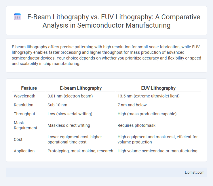
Table of Comparison
| Feature | E-beam Lithography | EUV Lithography |
|---|---|---|
| Wavelength | 0.01 nm (electron beam) | 13.5 nm (extreme ultraviolet light) |
| Resolution | Sub-10 nm | 7 nm and below |
| Throughput | Low (slow serial writing) | High (mass production capable) |
| Mask Requirement | Maskless direct writing | Requires photomask |
| Cost | Lower equipment cost, higher operational time cost | High equipment and mask cost, efficient for volume production |
| Application | Prototyping, mask making, research | High-volume semiconductor manufacturing |
Introduction to E-beam and EUV Lithography
E-beam lithography utilizes focused beams of electrons to create extremely precise patterns on semiconductor wafers, ideal for high-resolution mask making and prototyping. EUV lithography employs extreme ultraviolet light with a wavelength of 13.5 nm, enabling mass production of advanced semiconductor nodes below 7 nm. Your choice between these technologies depends on the required resolution, throughput, and application within semiconductor manufacturing.
Fundamentals of E-beam Lithography
E-beam lithography utilizes a focused beam of electrons to directly write patterns onto a resist-coated substrate with nanometer precision, enabling superior resolution compared to optical methods. This technique relies on electron scattering and resist exposure, where the electron beam induces chemical changes in a polymer resist, allowing selective removal during development. Despite its high-resolution capabilities, e-beam lithography is limited by slower throughput and patterning speed, making it ideal for mask making, prototyping, and research applications rather than high-volume semiconductor manufacturing.
Fundamentals of EUV Lithography
EUV lithography operates using extreme ultraviolet light with a wavelength of approximately 13.5 nanometers, enabling patterning of semiconductor features at the sub-7 nanometer scale. It relies on reflective optics and specialized photoresists to achieve high-resolution imaging, essential for advanced semiconductor manufacturing. Understanding these fundamentals helps you appreciate how EUV lithography overcomes limitations faced by traditional techniques like E-beam lithography.
Resolution Capabilities Comparison
E-beam lithography offers exceptional resolution capabilities, achieving features below 10 nanometers due to its precise electron beam control and direct-write technique, making it ideal for mask making and research applications. EUV lithography operates at a 13.5 nm wavelength, enabling high-throughput semiconductor manufacturing with resolutions around 7 nanometers, suitable for advanced logic and memory chip production. Despite EUV's faster processing speed, e-beam lithography remains superior in resolution for specialized, low-volume fabrication requiring ultra-fine patterns.
Throughput and Productivity Differences
E-beam lithography offers high resolution but suffers from low throughput due to its serial writing process, making it less productive for mass production. EUV lithography, utilizing a high-power light source and parallel patterning, significantly boosts throughput and productivity for advanced semiconductor manufacturing. Your choice depends on whether precision or volume is the priority, with EUV favored for large-scale chip fabrication.
Cost Analysis: E-beam vs EUV
E-beam lithography offers lower upfront equipment costs but suffers from slower throughput, leading to higher per-unit costs in mass production compared to EUV lithography. EUV lithography involves significant investment in complex light sources and masks, yet its high throughput and precision at nanometer-scale resolution reduce overall cost per wafer in large-volume semiconductor manufacturing. Cost analysis must weigh E-beam's suitability for prototyping and small-scale production against EUV's efficiency and scalability in advanced nodes like 5nm and below.
Application Areas and Use Cases
E-beam lithography excels in mask making, prototyping, and research applications requiring ultra-high resolution and custom patterning, particularly in semiconductor device fabrication and nanotechnology. EUV lithography dominates high-volume manufacturing of advanced integrated circuits, enabling mass production of chips with feature sizes below 7 nanometers due to its high throughput and precision. Both technologies support emerging uses such as photonic devices and quantum computing components, but EUV is preferred for large-scale commercial production while E-beam serves specialized, low-volume tasks demanding ultimate accuracy.
Technical Challenges in E-beam and EUV
E-beam lithography faces technical challenges such as slow throughput and electron scattering, which limit patterning speed and resolution uniformity on large wafers. EUV lithography struggles with source power limitations, mask defects, and the need for high-purity multilayer mirrors to maintain pattern fidelity. Both technologies require advanced resist materials and precise control systems to overcome stochastic effects and achieve sub-7nm node manufacturability.
Future Trends in Lithography Technologies
E-beam lithography continues to advance with improvements in beam control and multi-beam systems, enabling higher resolution patterning for niche applications like mask making and prototype development. EUV lithography is rapidly evolving with enhancements in source power and resist sensitivity, driving high-volume manufacturing at 3nm and beyond nodes. Future trends emphasize hybrid approaches integrating E-beam's precision with EUV's throughput to overcome scaling challenges and extend Moore's Law.
Conclusion: Choosing the Right Lithography Method
E-beam lithography offers high resolution and flexibility, making it ideal for prototyping and small-scale production, while EUV lithography delivers rapid throughput suited for mass manufacturing of advanced semiconductor devices. Your choice depends on factors such as device complexity, production volume, and cost constraints, as E-beam excels in precision without mask requirements whereas EUV enables high-volume, fine-feature patterning with higher initial investment. Evaluating these parameters ensures optimal alignment of lithography technology with your semiconductor fabrication goals.
E-beam Lithography vs EUV Lithography Infographic