Lithography involves creating patterns on a substrate using various techniques, while photolithography specifically uses light to transfer geometric shapes onto a photosensitive material. Your choice between lithography and photolithography depends on the precision and scale required for microfabrication processes.
Table of Comparison
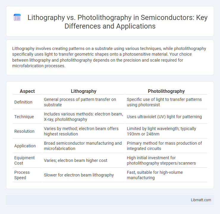
| Aspect | Lithography | Photolithography |
|---|---|---|
| Definition | General process of pattern transfer on substrate | Specific use of light to transfer patterns using photoresist |
| Technique | Includes various methods: electron beam, X-ray, photolithography | Uses ultraviolet (UV) light for patterning |
| Resolution | Varies by method; electron beam offers highest resolution | Limited by light wavelength; typically 193nm or 248nm |
| Application | Broad semiconductor manufacturing and microfabrication | Primary method for mass production of integrated circuits |
| Equipment Cost | Varies; electron beam higher cost | High initial investment for photolithography steppers/scanners |
| Process Speed | Slower for electron beam lithography | Fast, suitable for high-volume manufacturing |
Introduction to Lithography and Photolithography
Lithography is a technique used to transfer patterns onto a substrate, essential in microfabrication and printing. Photolithography, a subset of lithography, employs light to project intricate designs onto photosensitive materials, enabling precise circuit patterning in semiconductor manufacturing. Understanding the distinction between these processes helps you optimize fabrication methods for electronics and nanoscale devices.
Historical Background of Lithography
Lithography, invented by Alois Senefelder in 1796, originally involved writing on limestone with greasy ink to create printing plates, revolutionizing image reproduction. Photolithography evolved in the early 20th century, integrating photographic techniques to transfer images onto substrates, crucial for semiconductor manufacturing. The historical progression from traditional lithography to photolithography marks a significant technological advancement in precision and scalability for mass production processes.
Evolution from Lithography to Photolithography
The evolution from traditional lithography to photolithography marks a significant advancement in microfabrication technology, with photolithography enabling higher precision and scalability through the use of ultraviolet light to transfer intricate patterns onto semiconductor wafers. This transition improved resolution from micrometer-level features achievable by manual or mechanical lithography methods to nanometer-scale features essential for modern integrated circuits. Innovations such as deep ultraviolet (DUV) and extreme ultraviolet (EUV) lithography further enhanced patterning capabilities, driving the miniaturization and complexity of electronic components.
Basic Principles of Lithography
Lithography is a printing technique that transfers patterns onto a substrate using a resistant material to create a mask for subsequent processing, commonly used in semiconductor fabrication. Photolithography, a subset of lithography, uses light exposure to transfer geometric patterns from a photomask onto a photosensitive chemical photoresist on the substrate. The basic principle of photolithography involves coating the wafer with photoresist, exposing it to ultraviolet light through a photomask, and developing the image to define micro- or nanoscale circuit features.
Fundamentals of Photolithography
Photolithography is a precise semiconductor manufacturing process relying on light to transfer geometric patterns from a mask to a photosensitive resist on a substrate, enabling micro- to nanoscale feature creation. This technique involves key steps such as coating the wafer with photoresist, exposing it to ultraviolet light through a photomask, and developing the resist to reveal the patterned areas for subsequent etching or doping. Your understanding of photolithography fundamentals is essential for optimizing microfabrication in integrated circuit production and MEMS device fabrication.
Key Differences Between Lithography and Photolithography
Lithography and photolithography differ primarily in their processes and applications, with lithography encompassing various printing and patterning techniques using physical or chemical methods, while photolithography specifically employs light to transfer geometric patterns onto substrates. Photolithography offers higher precision and is crucial for semiconductor manufacturing, enabling feature sizes in the nanometer range, whereas traditional lithography is often used for larger-scale printing and microfabrication. Understanding these distinctions helps you select the appropriate technique for your project's resolution and scalability requirements.
Advantages and Limitations of Lithography
Lithography offers high precision and scalability suitable for diverse applications like semiconductor manufacturing and nano-fabrication, providing cost-effective patterning techniques. Its advantages include rapid processing speeds and the ability to create intricate patterns with high resolution. However, lithography faces limitations such as sensitivity to substrate materials, potential resolution constraints due to light diffraction limits, and the need for cleanroom environments to prevent defects.
Benefits and Challenges of Photolithography
Photolithography offers precise patterning essential for semiconductor manufacturing, enabling smaller feature sizes and higher circuit densities compared to traditional lithography. Your production benefits from increased resolution and scalability but faces challenges such as high equipment costs and sensitivity to light wavelength limitations. Managing defects and maintaining process control are critical to optimizing photolithography's advantages in microfabrication.
Applications in Modern Industry
Lithography and photolithography serve critical roles in modern industry, particularly in semiconductor manufacturing where photolithography enables the precise patterning of microchips using light exposure on photoresist materials. Traditional lithography techniques find applications in printing, graphic arts, and surface patterning on various substrates, supporting industries like packaging and textiles. Your understanding of these processes highlights their distinct advantages: photolithography's high resolution for integrated circuits and lithography's versatility for large-scale, cost-effective designs.
Future Trends and Innovations in Lithographic Techniques
Future trends in lithography emphasize extreme ultraviolet (EUV) and nanoimprint lithography techniques, significantly enhancing resolution beyond conventional photolithography limits. Innovations target increased precision in patterning sub-5 nm semiconductor nodes, enabling advancements in quantum computing and AI hardware. Integration of artificial intelligence and machine learning optimizes lithographic process controls, reducing defects and improving yield in mass semiconductor manufacturing.
Lithography vs Photolithography Infographic