PVD TiN coatings provide superior hardness and wear resistance due to their dense, crystalline structure, ideal for cutting tools and decorative finishes. ALD TiN offers excellent conformality and uniform thickness on complex geometries, making it perfect for intricate semiconductor and microelectronics applications where precise control is essential.
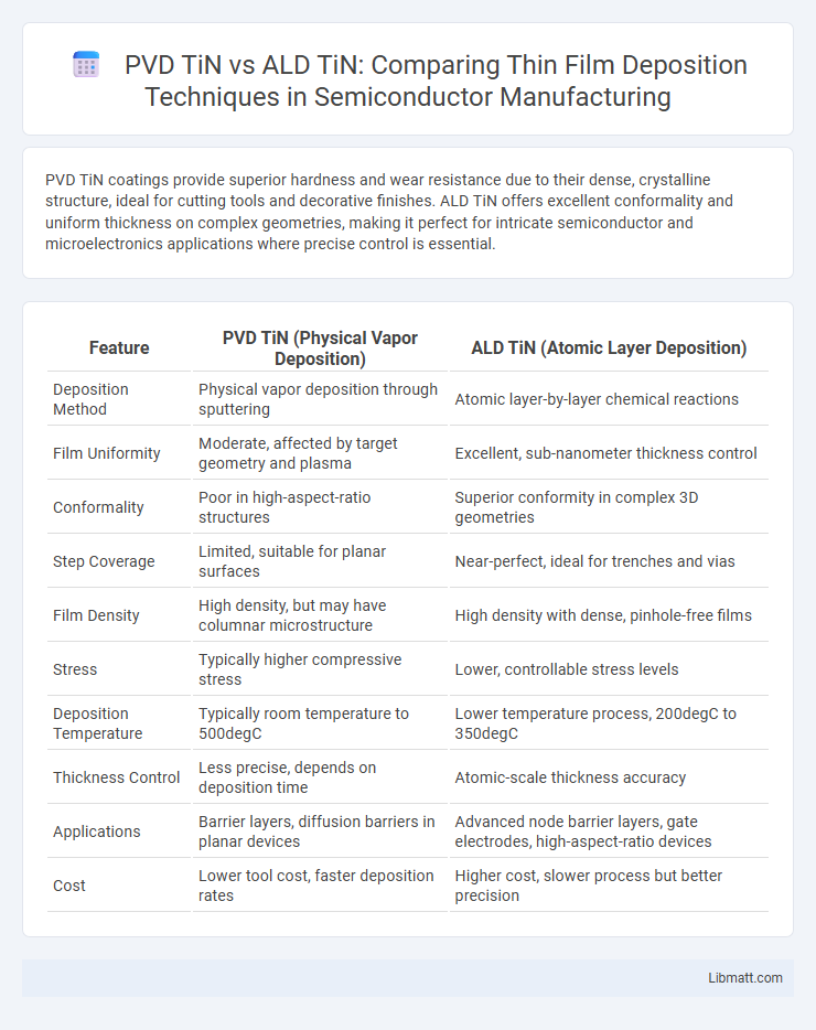
Table of Comparison
| Feature | PVD TiN (Physical Vapor Deposition) | ALD TiN (Atomic Layer Deposition) |
|---|---|---|
| Deposition Method | Physical vapor deposition through sputtering | Atomic layer-by-layer chemical reactions |
| Film Uniformity | Moderate, affected by target geometry and plasma | Excellent, sub-nanometer thickness control |
| Conformality | Poor in high-aspect-ratio structures | Superior conformity in complex 3D geometries |
| Step Coverage | Limited, suitable for planar surfaces | Near-perfect, ideal for trenches and vias |
| Film Density | High density, but may have columnar microstructure | High density with dense, pinhole-free films |
| Stress | Typically higher compressive stress | Lower, controllable stress levels |
| Deposition Temperature | Typically room temperature to 500degC | Lower temperature process, 200degC to 350degC |
| Thickness Control | Less precise, depends on deposition time | Atomic-scale thickness accuracy |
| Applications | Barrier layers, diffusion barriers in planar devices | Advanced node barrier layers, gate electrodes, high-aspect-ratio devices |
| Cost | Lower tool cost, faster deposition rates | Higher cost, slower process but better precision |
Introduction to TiN Coating Technologies
TiN coating technologies primarily include Physical Vapor Deposition (PVD) and Atomic Layer Deposition (ALD), each offering distinct benefits in hardness, adhesion, and uniformity. PVD TiN produces dense, hard coatings ideal for cutting tools with excellent wear resistance, while ALD TiN provides atomic-scale thickness control and conformal coverage on complex geometries. Your choice depends on the specific application requirements, such as coating precision or surface conformity.
Overview of PVD TiN Coating
PVD TiN coating offers a dense, hard surface layer with excellent abrasion resistance and a characteristic golden appearance, commonly used for cutting tools and decorative applications. This method deposits titanium nitride through physical vapor deposition, ensuring strong adhesion and uniform thickness on complex geometries. You benefit from improved tool life and reduced friction due to PVD TiN's superior hardness and thermal stability compared to other coating techniques.
Fundamentals of ALD TiN Coating
Atomic Layer Deposition (ALD) TiN coating utilizes sequential, self-limiting surface reactions to achieve ultra-thin, conformal, and highly uniform titanium nitride films, offering superior control at the atomic scale compared to Physical Vapor Deposition (PVD) TiN. ALD TiN exhibits excellent step coverage and excellent thickness uniformity on complex 3D structures, attributed to its layer-by-layer growth mechanism. This precise atomic control enhances film density, reduces defects, and improves corrosion resistance and electrical properties essential for advanced semiconductor and protective applications.
Deposition Process Comparison: PVD vs. ALD
Physical Vapor Deposition (PVD) TiN involves sputtering or evaporation techniques that deposit titanium nitride through high-energy particle bombardment, resulting in relatively fast film growth with moderate step coverage and density. Atomic Layer Deposition (ALD) TiN uses sequential, self-limiting surface chemical reactions to achieve atomic-scale control over film thickness, delivering superior conformality and uniformity, especially on complex 3D structures. Your choice between PVD and ALD for TiN coatings depends on the required film conformity, deposition rate, and application-specific surface topology.
Thickness and Uniformity Analysis
PVD TiN coatings typically exhibit thickness variations ranging from 1 to 5 microns, with moderate uniformity due to line-of-sight deposition methods that can cause shadowing effects on complex geometries. ALD TiN films achieve ultra-thin thickness control at the atomic scale, often below 100 nanometers, with exceptional uniformity across intricate 3D shapes due to its self-limiting surface reactions. This precise thickness control and conformality make ALD TiN ideal for applications requiring nanoscale coatings with consistent properties over high-aspect-ratio structures.
Adhesion and Mechanical Properties
PVD TiN (Physical Vapor Deposition Titanium Nitride) exhibits superior adhesion due to its high-density coating and strong interfacial bonding with substrates, making it ideal for wear-resistant applications. ALD TiN (Atomic Layer Deposition Titanium Nitride) provides excellent thickness uniformity and conformality but generally shows lower mechanical strength and adhesion compared to PVD. Mechanical properties of PVD TiN include higher hardness and better resistance to abrasion, whereas ALD TiN offers enhanced control over film composition and thickness at the atomic level, which can be advantageous for specific nanoscale applications.
Electrical and Chemical Properties
PVD TiN (Physical Vapor Deposition Titanium Nitride) exhibits higher electrical conductivity due to its dense and crystalline microstructure, making it ideal for applications requiring low resistivity. ALD TiN (Atomic Layer Deposition Titanium Nitride) offers superior chemical uniformity and conformality with enhanced corrosion resistance and better barrier properties due to its atomic-scale thickness control. The chemical stability of ALD TiN outperforms PVD TiN, especially under harsh chemical environments, while PVD TiN provides more efficient electrical pathways in microelectronics.
Applications in Industry: PVD TiN vs. ALD TiN
PVD TiN coatings are commonly used in cutting tools, molds, and aerospace components due to their excellent hardness and wear resistance, ideal for high-stress environments. ALD TiN offers superior conformality and uniform thickness, making it crucial for semiconductor devices, microelectronics, and complex 3D structures in advanced industrial applications. Your choice between PVD and ALD TiN depends on whether you prioritize bulk mechanical performance or precision thin-film deposition for intricate geometries.
Cost and Scalability Considerations
PVD TiN typically offers lower initial equipment costs and faster deposition rates, making it more cost-effective for large-scale production runs. ALD TiN provides superior film conformality and thickness control but involves higher operational expenses and slower throughput, impacting scalability for high-volume manufacturing. Choosing the right technique depends on Your application's balance between cost constraints and scalability requirements.
Choosing the Right TiN Coating Method
Choosing the right TiN coating method depends on your application's precision and durability requirements. PVD TiN offers excellent adhesion and hardness for tools and cutting edges, while ALD TiN provides superior conformality and uniform thickness on complex, high-aspect-ratio structures. Understanding these differences ensures your coating process maximizes performance, wear resistance, and longevity in your specific use case.
PVD TiN vs ALD TiN Infographic