Etch residue consists of inorganic byproducts left on a surface after an etching process, often requiring specific chemical cleaners for removal, while organic residue is composed of carbon-based compounds such as photoresist remnants that typically dissolve in organic solvents. Understanding the differences between etch residue and organic residue is crucial for selecting the appropriate cleaning method to ensure optimal surface preparation and device performance.
Table of Comparison
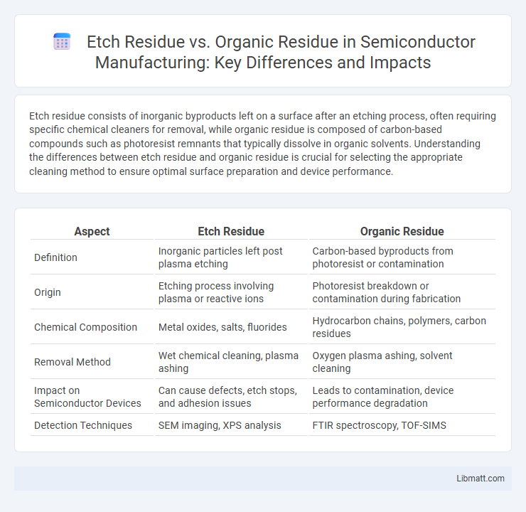
| Aspect | Etch Residue | Organic Residue |
|---|---|---|
| Definition | Inorganic particles left post plasma etching | Carbon-based byproducts from photoresist or contamination |
| Origin | Etching process involving plasma or reactive ions | Photoresist breakdown or contamination during fabrication |
| Chemical Composition | Metal oxides, salts, fluorides | Hydrocarbon chains, polymers, carbon residues |
| Removal Method | Wet chemical cleaning, plasma ashing | Oxygen plasma ashing, solvent cleaning |
| Impact on Semiconductor Devices | Can cause defects, etch stops, and adhesion issues | Leads to contamination, device performance degradation |
| Detection Techniques | SEM imaging, XPS analysis | FTIR spectroscopy, TOF-SIMS |
Introduction to Etch Residue and Organic Residue
Etch residue and organic residue are common contaminants encountered during semiconductor manufacturing and PCB fabrication. Etch residue forms as a byproduct of the chemical etching process, consisting mainly of inorganic compounds, while organic residue originates from photoresist materials and other organic compounds used in lithography. Understanding the differences between etch residue and organic residue is essential for optimizing cleaning processes and ensuring the integrity of your microelectronic devices.
Defining Etch Residue
Etch residue is the unwanted material left on a substrate surface after the completion of an etching process, typically formed from the reaction by-products of the etching chemicals and the substrate materials. Unlike organic residue, which consists primarily of carbon-based contaminants such as photoresist or adhesive remnants, etch residue often includes inorganic compounds like salts, oxides, or polymers resulting from plasma or wet etch reactions. Proper identification and removal of etch residue are critical in semiconductor manufacturing to ensure device performance and prevent defects during subsequent fabrication steps.
Defining Organic Residue
Organic residue refers to carbon-based materials left behind after chemical or physical processing, often resulting from photoresist polymers or contaminants in semiconductor fabrication. Unlike etch residue, which typically consists of inorganic byproducts formed during etching processes, organic residue can interfere with device performance by causing contamination or adhesion issues. Understanding the nature of organic residue helps you optimize cleaning and surface preparation steps to ensure high-quality microfabrication outcomes.
Chemical Composition Differences
Etch residue primarily consists of inorganic compounds such as metal oxides and fluoride salts formed during plasma or wet etching processes, whereas organic residue is composed mainly of carbon-based byproducts like polymers and photoresist fragments. The chemical composition differences are crucial for selecting appropriate cleaning techniques, as inorganic etch residues require acid or base treatments, while organic residues often need solvent or plasma-based removal methods. Understanding your substrate's contamination profile helps optimize residue elimination and maintain surface integrity.
Sources and Formation Processes
Etch residue originates from the physical or chemical reaction between the etching plasma or chemicals and the substrate material, often involving materials like silicon, silicon dioxide, or metals. Organic residue forms from incomplete removal of polymeric materials, photoresists, or contamination involving carbon-based compounds during semiconductor fabrication. Understanding the distinct formation processes is crucial for optimizing cleaning techniques and improving device yield in microfabrication.
Impact on Semiconductor Manufacturing
Etch residue, composed of inorganic materials such as metal oxides or polymers, can cause defects in semiconductor devices by creating uneven surfaces and compromising layer adhesion. Organic residue, typically resulting from photoresist remnants or polymer side products, affects device performance by contaminating critical interfaces and causing variations in electrical properties. Managing both types of residues is essential for maintaining yield, ensuring circuit reliability, and optimizing your semiconductor manufacturing process.
Detection and Analysis Methods
Etch residue and organic residue are distinguished through advanced detection and analysis methods such as scanning electron microscopy (SEM) combined with energy-dispersive X-ray spectroscopy (EDX) for precise elemental identification. Fourier-transform infrared spectroscopy (FTIR) and Raman spectroscopy provide detailed molecular characterization of organic residues, while X-ray photoelectron spectroscopy (XPS) offers surface chemical composition crucial for etch residue analysis. You can achieve accurate differentiation by employing these complementary techniques, ensuring proper identification and effective removal strategies in semiconductor manufacturing processes.
Removal Techniques for Each Residue
Etch residue removal techniques involve wet chemical cleaning using solutions like hydrofluoric acid or specialized solvents that dissolve inorganic deposits formed during plasma etching. Organic residue, often consisting of polymerized photoresist or carbon-based films, is effectively removed with oxygen plasma ashing or solvent-based strippers designed to break down complex hydrocarbons. Selecting the optimal removal method ensures your semiconductor fabrication processes maintain surface integrity and prevent contamination-related yield loss.
Challenges in Residue Management
Etch residue management faces challenges due to the complex chemical composition and adhesion properties that differ significantly from organic residue, which primarily consists of carbon-based contaminants requiring different cleaning approaches. Etch residues often consist of inorganic byproducts like metal fluorides or oxides that are chemically stable and may require aggressive plasma or wet etching processes, whereas organic residues demand specialized solvent or ashing treatments to prevent polymer buildup. Effective residue removal must balance process parameters to avoid substrate damage while ensuring complete elimination of both inorganic etch residues and organic contaminants, which can impair device performance and yield.
Best Practices for Residue Prevention
Effective residue prevention in semiconductor manufacturing centers on selecting precise etching parameters and proper cleaning protocols. Etch residue often results from ion bombardment and polymer buildup, while organic residue stems from photoresist or contaminant degradation, making tailored chemical treatments essential. Ensuring your process employs optimized gas mixtures, controlled plasma power, and timely wet cleans reduces both etch and organic residues, enhancing device yield and performance.
Etch Residue vs Organic Residue Infographic