Planar transistors have a flat structure where current flows horizontally, resulting in simpler manufacturing but facing limitations in scaling and power efficiency. FinFETs feature a 3D fin-like structure that enhances electrostatic control and reduces leakage, significantly improving your device's performance and power consumption in advanced semiconductor technologies.
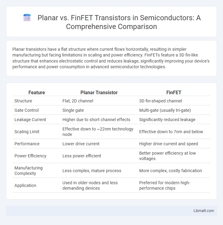
Table of Comparison
| Feature | Planar Transistor | FinFET |
|---|---|---|
| Structure | Flat, 2D channel | 3D fin-shaped channel |
| Gate Control | Single gate | Multi-gate (usually tri-gate) |
| Leakage Current | Higher due to short channel effects | Significantly reduced leakage |
| Scaling Limit | Effective down to ~22nm technology node | Effective down to 7nm and below |
| Performance | Lower drive current | Higher drive current and speed |
| Power Efficiency | Less power efficient | Better power efficiency at low voltages |
| Manufacturing Complexity | Less complex, mature process | More complex, costly fabrication |
| Application | Used in older nodes and less demanding devices | Preferred for modern high-performance chips |
Introduction to Planar and FinFET Technologies
Planar and FinFET technologies represent two generations of transistor design fundamental to semiconductor manufacturing. Planar transistors feature a flat channel for current flow, widely used in earlier technology nodes up to 22nm. FinFET, or Fin Field-Effect Transistor, introduces a three-dimensional fin-shaped channel structure, enhancing control over short-channel effects and enabling improved performance and lower power consumption at advanced nodes of 14nm and below.
Historical Evolution of Semiconductor Transistors
The historical evolution of semiconductor transistors transitioned from planar transistors, which dominated the industry for decades due to their simple fabrication and reliable performance, to FinFET technology designed to overcome planar scaling limitations. FinFETs introduced a 3D structure that significantly improved control over short-channel effects, enhancing power efficiency and speed as transistor dimensions shrank below 22 nanometers. Your devices now benefit from FinFET advancements, which represent a critical shift enabling continued semiconductor scaling and innovation beyond the constraints of planar designs.
Structural Differences: Planar vs. FinFET
Planar transistors feature a flat, two-dimensional channel where current flows horizontally between the source and drain beneath the gate, while FinFETs utilize a three-dimensional fin-shaped channel that rises vertically from the substrate, providing better electrostatic control. The 3D structure of FinFETs reduces short-channel effects and leakage currents, enhancing performance and power efficiency compared to the planar design. Understanding these structural differences helps you appreciate why FinFET technology dominates advanced semiconductor manufacturing nodes.
Performance Comparison: Speed, Power, and Efficiency
FinFET technology exhibits superior performance compared to planar transistors, offering significantly higher switching speeds due to its 3D structure that improves gate control and reduces short-channel effects. Power consumption is substantially lower in FinFET devices, as they minimize leakage current and enable efficient voltage scaling, which enhances overall energy efficiency. The advanced architecture of FinFETs results in improved transistor density and thermal management, making them more efficient for high-performance integrated circuits compared to traditional planar designs.
Scaling Challenges in Modern Transistor Architectures
Planar transistors face significant scaling challenges due to short-channel effects and leakage currents as channel lengths shrink below 20nm, limiting performance and power efficiency. FinFET architectures mitigate these issues with a 3D multi-gate structure that provides better electrostatic control, enabling continued scaling down to sub-5nm nodes. The transition from planar to FinFET has been critical in sustaining Moore's Law by improving drive current and reducing off-state leakage in advanced semiconductor manufacturing.
Manufacturing Complexity and Costs
Planar transistors feature simpler, more mature manufacturing processes, resulting in lower fabrication costs compared to FinFETs. FinFET technology involves complex 3D structure fabrication with advanced lithography and etching steps, increasing production complexity and expense. Your choice between the two impacts both device performance and overall manufacturing budgets due to these cost and process differences.
Reliability and Heat Dissipation
FinFET technology offers superior reliability compared to planar transistors due to its three-dimensional structure, which reduces leakage currents and improves electrostatic control. Heat dissipation is more efficient in FinFETs because their vertical fins increase surface area, allowing better thermal management under high-performance conditions. Your choice between planar and FinFET impacts device longevity and temperature stability, with FinFETs generally delivering enhanced performance in these critical areas.
Adoption in Industry: Mainstream Applications
Planar transistors dominated semiconductor manufacturing until the shift toward FinFET technology, which now leads in mainstream applications due to superior performance at smaller nodes like 7nm and below. FinFET adoption accelerates in high-performance computing, mobile processors, and AI chips, offering reduced leakage current and enhanced energy efficiency compared to planar designs. Your choice between planar and FinFET transistors impacts device power consumption and scaling potential in advanced integrated circuits.
Future Trends in Transistor Design
FinFET technology continues to dominate advanced semiconductor manufacturing due to superior control over short-channel effects and reduced leakage currents compared to planar transistors. Emerging transistor designs, such as Gate-All-Around (GAA) and nanosheet transistors, aim to build on FinFET's 3D architecture by further enhancing electrostatic control and scaling beyond 3nm nodes. Industry leaders like TSMC and Samsung are investing heavily in GAA transistor development to meet growing demands for power efficiency and performance in next-generation integrated circuits.
Conclusion: Choosing the Right Technology
Planar and FinFET technologies each offer distinct advantages depending on performance and power efficiency requirements. Planar transistors remain cost-effective for lower power applications and simpler designs, while FinFETs deliver superior scaling, reduced leakage, and enhanced speed critical for advanced nodes below 20nm. Selecting the right technology hinges on balancing manufacturing complexity, device performance, and overall system goals to optimize semiconductor design.
Planar vs FinFET Infographic