Blanket deposition uniformly coats an entire substrate, ideal for creating consistent thin films over large areas, while selective deposition targets specific regions, enhancing precision and material efficiency in device fabrication. Understanding these methods helps optimize your manufacturing process by balancing coverage needs with material usage.
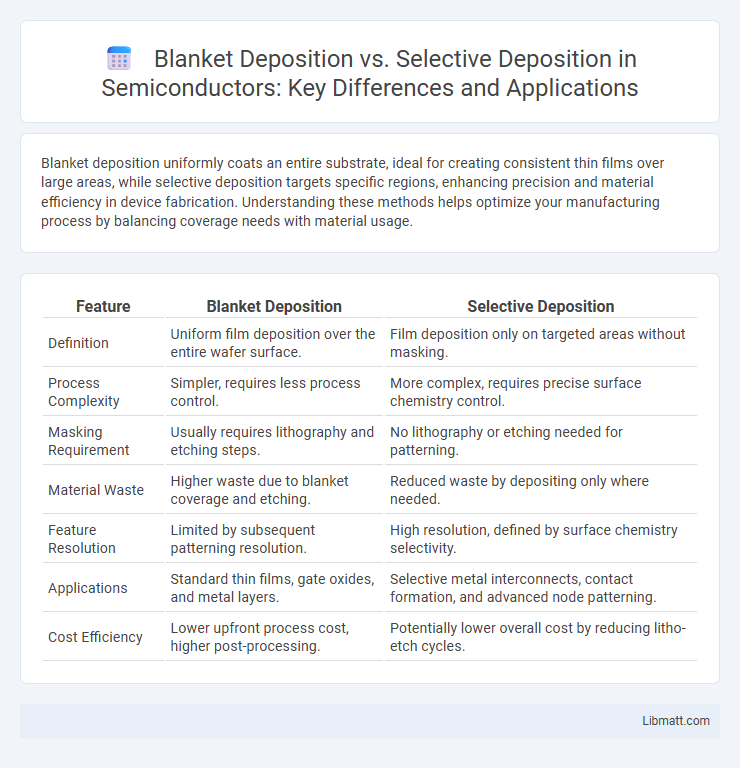
Table of Comparison
| Feature | Blanket Deposition | Selective Deposition |
|---|---|---|
| Definition | Uniform film deposition over the entire wafer surface. | Film deposition only on targeted areas without masking. |
| Process Complexity | Simpler, requires less process control. | More complex, requires precise surface chemistry control. |
| Masking Requirement | Usually requires lithography and etching steps. | No lithography or etching needed for patterning. |
| Material Waste | Higher waste due to blanket coverage and etching. | Reduced waste by depositing only where needed. |
| Feature Resolution | Limited by subsequent patterning resolution. | High resolution, defined by surface chemistry selectivity. |
| Applications | Standard thin films, gate oxides, and metal layers. | Selective metal interconnects, contact formation, and advanced node patterning. |
| Cost Efficiency | Lower upfront process cost, higher post-processing. | Potentially lower overall cost by reducing litho-etch cycles. |
Introduction to Deposition Techniques
Blanket deposition uniformly coats the entire surface of a substrate, making it ideal for creating consistent thin films in semiconductor manufacturing. Selective deposition targets specific areas, allowing precise material placement without the need for additional patterning or etching steps. Understanding these techniques is crucial for optimizing your fabrication process and achieving desired device performance.
What is Blanket Deposition?
Blanket deposition is a process used in semiconductor manufacturing where a thin film is uniformly deposited over the entire surface of a wafer, covering all areas regardless of the underlying materials or patterns. This technique ensures consistent layer thickness and material coverage, which is crucial for creating uniform electrical and physical properties across the chip. Your choice between blanket deposition and selective deposition depends on the specific device architecture and process requirements.
What is Selective Deposition?
Selective deposition is a precise thin-film coating technique where material is deposited only on specific areas of a substrate, avoiding unnecessary coverage and reducing the need for subsequent etching processes. This method enhances manufacturing efficiency by targeting deposition to desired regions, improving film quality and minimizing waste compared to blanket deposition, which applies a uniform layer over the entire surface. Your production line benefits from selective deposition through higher accuracy and decreased material usage in semiconductor fabrication and electronics manufacturing.
Key Differences Between Blanket and Selective Deposition
Blanket deposition uniformly coats the entire substrate surface with a thin film, ensuring consistent layer thickness across all areas, while selective deposition targets specific regions, avoiding unwanted coating and reducing material waste. In semiconductor fabrication, blanket deposition is advantageous for creating uniform dielectric or metal layers, whereas selective deposition enhances pattern precision and device performance by eliminating the need for additional etching steps. The choice between these methods hinges on process complexity, cost efficiency, and the desired structural accuracy in microfabrication.
Advantages of Blanket Deposition
Blanket deposition offers uniform thin film coverage over the entire substrate, making it ideal for consistent layer formation in semiconductor manufacturing. This method enhances process simplicity and throughput by avoiding complex patterning steps required in selective deposition. Its ability to produce conformal coatings on various topographies improves device reliability and yield.
Advantages of Selective Deposition
Selective deposition offers enhanced process efficiency by directly applying materials only to desired areas, reducing waste and contamination compared to blanket deposition. This targeted approach improves device performance by minimizing undesired film formation and simplifying patterning steps. Selective deposition also enables finer feature control and scalability for advanced semiconductor manufacturing.
Applications in Semiconductor Manufacturing
Blanket deposition uniformly coats entire semiconductor wafers, making it ideal for creating thin films and dielectric layers essential in transistor fabrication and insulating layers. Selective deposition targets specific regions, enabling precise material placement for gate electrodes and contact pads, reducing processing steps and material waste. Your choice between these techniques impacts device performance, yield, and manufacturing cost efficiency in semiconductor production.
Challenges and Limitations of Each Method
Blanket deposition faces challenges such as uniform film thickness over complex topographies and increased material waste, limiting efficiency in intricate device fabrication. Selective deposition struggles with achieving high selectivity without defects or contamination, often requiring precise surface treatments and increasing process complexity. Your choice depends on balancing these limitations against specific application requirements and manufacturing capabilities.
Recent Advances in Deposition Technologies
Recent advances in deposition technologies have significantly enhanced the precision and efficiency of both blanket deposition and selective deposition processes. Blanket deposition techniques, such as atomic layer deposition (ALD), now offer improved uniformity and conformality over large substrates, enabling better control at the nanoscale. Selective deposition methods have progressed with innovations like area-selective ALD and plasma-enhanced chemical vapor deposition (PECVD), allowing your fabrication processes to target specific regions without masking steps, reducing complexity and material waste.
Future Trends in Deposition Methods
Future trends in blanket deposition emphasize uniform thin-film layers for large-scale applications like semiconductor wafers, enhancing reproducibility and efficiency. Selective deposition advances target precision in patterning and material placement, crucial for next-generation microelectronics and quantum devices. Your choice between these methods will depend on the balance of scalability and feature-specific requirements in emerging technologies.
Blanket Deposition vs Selective Deposition Infographic