The Redistribution Layer (RDL) provides an additional routing layer in advanced semiconductor packaging, enabling denser interconnects and improved electrical performance, whereas the Re-Distribution Layer (RDL) typically refers to a similar concept but can sometimes be used interchangeably or contextually in packaging design. Understanding the differences in terminology and application can help optimize your chip design for better signal integrity and package integration.
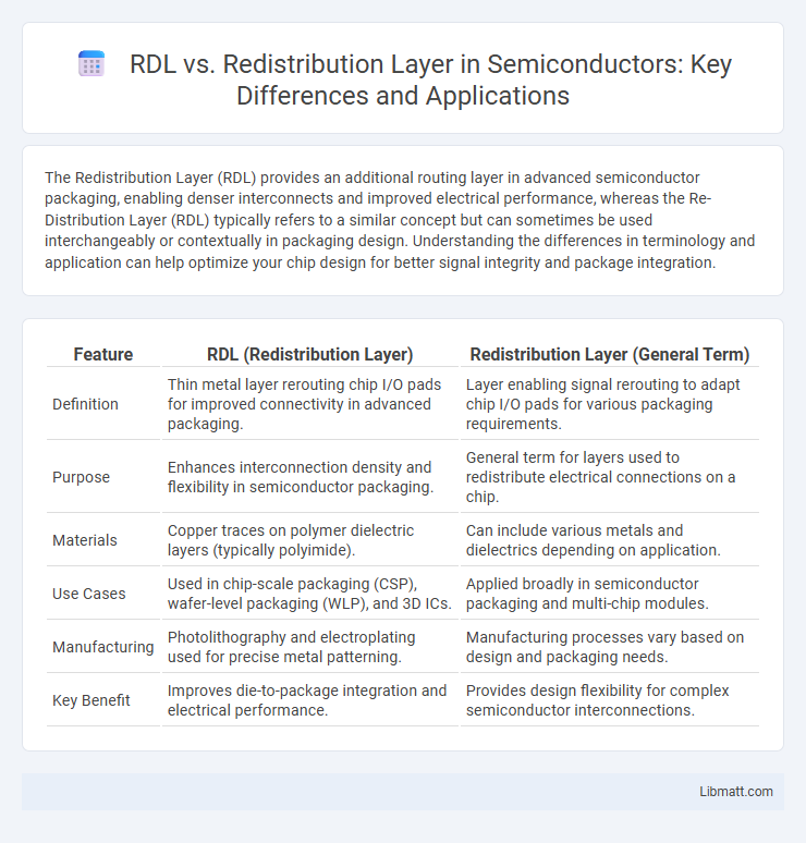
Table of Comparison
| Feature | RDL (Redistribution Layer) | Redistribution Layer (General Term) |
|---|---|---|
| Definition | Thin metal layer rerouting chip I/O pads for improved connectivity in advanced packaging. | Layer enabling signal rerouting to adapt chip I/O pads for various packaging requirements. |
| Purpose | Enhances interconnection density and flexibility in semiconductor packaging. | General term for layers used to redistribute electrical connections on a chip. |
| Materials | Copper traces on polymer dielectric layers (typically polyimide). | Can include various metals and dielectrics depending on application. |
| Use Cases | Used in chip-scale packaging (CSP), wafer-level packaging (WLP), and 3D ICs. | Applied broadly in semiconductor packaging and multi-chip modules. |
| Manufacturing | Photolithography and electroplating used for precise metal patterning. | Manufacturing processes vary based on design and packaging needs. |
| Key Benefit | Improves die-to-package integration and electrical performance. | Provides design flexibility for complex semiconductor interconnections. |
Introduction to RDL and Redistribution Layer
RDL (Redistribution Layer) refers to an intermediate layer of wiring in semiconductor packaging, enabling rerouting of I/O pads to match different package designs and facilitating higher-density interconnections. The Redistribution Layer improves electrical performance and manufacturing flexibility by relocating input/output contacts from the silicon chip to the package substrate. Your device's chip functionality and packaging efficiency benefit significantly from the integration of RDL in advanced electronics assembly.
What Is RDL (Redistribution Layer) in Semiconductor Manufacturing?
RDL (Redistribution Layer) in semiconductor manufacturing refers to an additional metallization layer used to reroute the I/O pads of an integrated circuit to a different layout or pitch, enabling better connectivity and integration with other components. This layer is critical for advanced packaging technologies such as wafer-level packaging (WLP) and system-in-package (SiP), facilitating improved electrical performance and miniaturization. Key materials for RDL include copper or aluminum, deposited using photolithography to create precise interconnect patterns that enhance chip functionality and reliability.
Key Functions of RDL vs Traditional Redistribution Layers
RDL (Redistribution Layer) enhances semiconductor packaging by providing finer pitch routing, improved electrical performance, and better integration capabilities compared to traditional Redistribution Layers, which primarily focus on basic fan-out of I/O pads. RDL supports advanced packaging technologies like 2.5D and 3D integration, allowing for complex signal routing and high-density interconnections, whereas traditional layers are limited in scalability and flexibility. Your choice of RDL technology can significantly impact device performance, signal integrity, and overall system miniaturization.
RDL Process Flow and Technology Overview
The Redistribution Layer (RDL) process involves wafer-level packaging technology that reroutes I/O pads to a new pattern for improved interconnect density and device integration. Advanced photolithography and electroplating techniques form metal traces on the dielectric layers, ensuring precision in micro-scale rerouting. Your semiconductor designs benefit from enhanced electrical performance and layout flexibility through this critical RDL technology.
Types of RDL: Single-Layer vs Multi-Layer
Single-layer RDL offers a straightforward redistribution path, ideal for simpler packaging designs with limited routing complexity. Multi-layer RDL enhances routing density and signal integrity by stacking multiple metal layers, enabling advanced interconnect solutions for high-performance devices. Your choice between single-layer and multi-layer RDL depends on the complexity of the package and the required electrical performance.
Applications and Use Cases of RDL Technology
Redistribution Layer (RDL) technology is widely applied in advanced semiconductor packaging to reroute I/O pads, enabling higher-density interconnections and enhancing chip-to-package integration. Key use cases include system-in-package (SiP) designs, 3D IC stacking, and wafer-level packaging, where RDL minimizes signal loss and supports heterogeneous integration of multiple dies. RDL also enables fine-pitch routing for mobile devices, automotive electronics, and high-performance computing applications requiring compact, reliable, and high-speed connections.
Advantages of RDL over Conventional Redistribution Layers
RDL offers superior electrical performance and enhanced routing density compared to conventional redistribution layers, enabling more compact and efficient semiconductor packaging. Its improved planarization and lower defect rates increase overall device reliability and yield, benefiting advanced integrated circuits and system-in-package (SiP) solutions. By choosing RDL, your designs achieve higher interconnect integrity and support finer pitch layouts, optimizing both performance and manufacturability.
Challenges and Limitations in RDL Implementation
RDL (Redistribution Layer) implementation faces challenges such as precise alignment requirements and increased fabrication complexity, which can lead to higher manufacturing costs and yield loss. Signal integrity issues, including crosstalk and impedance discontinuities, also limit RDL performance in high-density designs. Understanding these limitations helps you optimize layout strategies and improve overall system reliability.
RDL in Advanced Packaging: Fan-Out and Fan-In Approaches
RDL (Redistribution Layer) plays a critical role in advanced packaging techniques such as fan-out and fan-in wafer-level packaging by enabling finer pitch routing and improved electrical performance. In fan-out packaging, RDL extends the I/O connections beyond the chip footprint, enhancing integration density and thermal management. Your devices benefit from optimized signal integrity and reduced package size through the precise implementation of redistribution layers.
Future Trends and Innovations in Redistribution Layer Technology
Redistribution Layer (RDL) technology is evolving rapidly to support higher density interconnects and improved signal integrity for advanced semiconductor packaging, addressing the increasing demands of 3D ICs and heterogeneous integration. Innovations such as finer pitch routing, advanced materials like graphene and nano copper, and enhanced thermal management techniques are set to revolutionize your chip design capabilities. Future trends also include AI-driven design automation and flexible RDLs enabling next-generation wearable and IoT devices with superior performance and reliability.
RDL vs Redistribution Layer Infographic