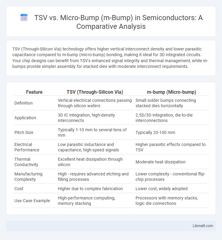
TSV (Through-Silicon Via) technology offers higher vertical interconnect density and lower parasitic capacitance compared to m-bump (micro-bump) bonding, making it ideal for 3D integrated circuits. Your chip designs can benefit from TSV's enhanced signal integrity and thermal management, while m-bumps provide simpler assembly for stacked dies with moderate interconnect requirements.
Table of Comparison
| Feature | TSV (Through-Silicon Via) | m-bump (Micro-bump) |
|---|---|---|
| Definition | Vertical electrical connections passing through silicon wafers | Small solder bumps connecting stacked dies horizontally |
| Application | 3D IC integration, high-density interconnects | 2.5D/3D integration, die-to-die interconnections |
| Pitch Size | Typically 1-10 mm to several tens of mm | Typically 20-100 mm |
| Electrical Performance | Low parasitic inductance and capacitance, high-speed signals | Higher parasitic effects compared to TSV |
| Thermal Conductivity | Excellent heat dissipation through silicon | Moderate heat dissipation |
| Manufacturing Complexity | High - requires advanced etching and filling processes | Lower complexity - conventional flip-chip processes |
| Cost | Higher due to complex fabrication | Lower cost, widely adopted |
| Use Case Example | High-performance computing, memory stacking | Processors with memory stacks, logic die connections |
Introduction to TSV and μ-bump Technologies
TSV (Through-Silicon Via) technology creates vertical electrical connections by drilling holes through silicon wafers, enabling high-density 3D integration in semiconductor devices. m-bump (micro-bump) technology forms small solder bumps used for chip-to-chip or chip-to-substrate interconnections, essential in advanced packaging for fine-pitch connections. Understanding the differences between TSV and m-bump helps optimize your design for performance, scalability, and manufacturing cost in modern electronics.
Fundamental Differences: TSV vs μ-bump
TSV (Through-Silicon Via) involves vertical electrical connections passing through the silicon substrate, enabling high-density 3D integration and improved performance in semiconductor devices. In contrast, m-bumps (micro-bumps) serve as tiny solder interconnects primarily used for die-to-die or die-to-substrate bonding in flip-chip packaging, facilitating mechanical and electrical connections without penetrating the silicon. Your choice between TSV and m-bump interconnects depends on factors like integration complexity, thermal management, and electrical performance requirements.
Applications in Modern Semiconductor Packaging
TSV (Through-Silicon Via) technology enables vertical electrical connections in 3D integrated circuits, enhancing performance in high-density memory and advanced logic chips used in smartphones and data centers. m-bump (micro-bump) interconnects serve as small solder bumps for fine-pitch chip-to-chip bonding, critical in high-speed packaging like HBM (High Bandwidth Memory) and advanced system-in-package (SiP) solutions. Your choice between TSV and m-bump depends on specific requirements such as signal integrity, thermal management, and package complexity in modern semiconductor applications.
Electrical Performance Comparison
TSV (Through-Silicon Via) technology offers lower parasitic capacitance and resistance compared to m-bump interconnections, resulting in enhanced signal integrity and reduced power consumption. m-bumps exhibit higher inductance and resistance due to their larger size and longer current paths, which can limit high-frequency performance. Optimizing your design with TSVs improves electrical performance in 3D integrated circuits by minimizing signal delay and crosstalk.
Impact on Signal Integrity and Bandwidth
TSV (Through-Silicon Via) technology enhances signal integrity by providing low-resistance, short interconnects that minimize parasitic inductance and capacitance, thereby supporting higher bandwidth in 3D integrated circuits. In contrast, m-bump (micro-bump) interconnections exhibit higher impedance and longer signal paths that can introduce more signal attenuation and crosstalk, limiting bandwidth and performance at high frequencies. Optimizing TSV dimensions and pitch is critical to maximizing bandwidth and maintaining signal fidelity in advanced semiconductor packaging.
Thermal Management Considerations
Through-silicon vias (TSVs) provide superior thermal conductivity compared to m-bumps due to their larger cross-sectional area and direct vertical heat dissipation paths within 3D integrated circuits. TSVs facilitate more efficient heat spreading and reduced hotspot formation, crucial for high-power semiconductor applications. In contrast, m-bumps exhibit higher thermal resistance, which can lead to thermal bottlenecks and potential reliability issues under intense operating conditions.
Integration Challenges and Solutions
Integration challenges of TSV (Through-Silicon Via) and m-bump (micro-bump) technologies primarily involve maintaining signal integrity, thermal management, and mechanical reliability. TSVs face complex fabrication processes and require advanced alignment techniques to ensure precise vertical interconnections in 3D IC stacks, while m-bumps face challenges in achieving uniform size and pitch for reliable flip-chip bonding. Solutions include using advanced lithography and etching methods for TSVs, and employing controlled reflow and inspection techniques for m-bump fabrication to enhance electrical performance and yield.
Cost Analysis: TSV vs μ-bump
Cost analysis between Through-Silicon Via (TSV) and micro-bump (m-bump) interconnect technologies reveals that TSV generally incurs higher fabrication expenses due to complex deep silicon etching and wafer bonding processes. Micro-bump technology offers a more cost-effective alternative with simpler manufacturing steps and compatibility with existing flip-chip assembly lines, significantly reducing overall packaging costs. Despite TSV's performance benefits in power and signal integrity, the substantial increase in processing time and specialized equipment often makes m-bump the preferred choice for cost-sensitive 3D integration applications.
Future Trends in 3D Packaging Interconnects
Future trends in 3D packaging interconnects highlight the evolution from traditional Through-Silicon Vias (TSVs) to advanced m-bump technologies, driven by the demand for higher density, improved electrical performance, and reduced form factors. TSVs offer vertical electrical connections through the silicon substrate, enabling efficient heat dissipation and signal integrity, while m-bumps serve as fine-pitched solder connections that facilitate dense chip stacking and enhanced mechanical reliability. Your selection between TSV and m-bump will significantly impact the scalability and performance of next-generation semiconductor devices.
Choosing the Right Technology for Your Application
TSV (Through-Silicon Via) and m-bump (micro-bump) technologies serve critical roles in 3D IC integration, with TSV offering high-density vertical interconnections suitable for complex, high-performance applications requiring low latency and enhanced electrical performance. m-bump technology excels in wafer-level packaging and is ideal for applications where cost efficiency and smaller form factors are priorities without the need for the deepest vertical integration. Your choice depends on performance requirements, thermal management needs, and budget constraints, ensuring the selected technology aligns with the specific demands of your application.
TSV vs μ-bump Infographic