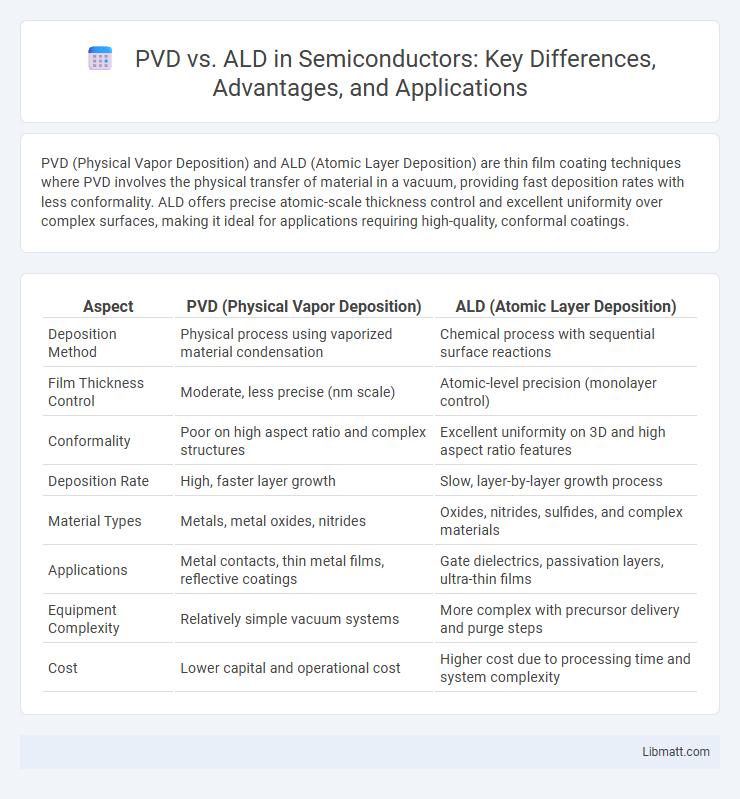
PVD (Physical Vapor Deposition) and ALD (Atomic Layer Deposition) are thin film coating techniques where PVD involves the physical transfer of material in a vacuum, providing fast deposition rates with less conformality. ALD offers precise atomic-scale thickness control and excellent uniformity over complex surfaces, making it ideal for applications requiring high-quality, conformal coatings.
Table of Comparison
| Aspect | PVD (Physical Vapor Deposition) | ALD (Atomic Layer Deposition) |
|---|---|---|
| Deposition Method | Physical process using vaporized material condensation | Chemical process with sequential surface reactions |
| Film Thickness Control | Moderate, less precise (nm scale) | Atomic-level precision (monolayer control) |
| Conformality | Poor on high aspect ratio and complex structures | Excellent uniformity on 3D and high aspect ratio features |
| Deposition Rate | High, faster layer growth | Slow, layer-by-layer growth process |
| Material Types | Metals, metal oxides, nitrides | Oxides, nitrides, sulfides, and complex materials |
| Applications | Metal contacts, thin metal films, reflective coatings | Gate dielectrics, passivation layers, ultra-thin films |
| Equipment Complexity | Relatively simple vacuum systems | More complex with precursor delivery and purge steps |
| Cost | Lower capital and operational cost | Higher cost due to processing time and system complexity |
Introduction to PVD and ALD
Physical Vapor Deposition (PVD) and Atomic Layer Deposition (ALD) are advanced thin film coating techniques used in semiconductor manufacturing and surface engineering. PVD involves the physical transfer of material from a source to a substrate, creating thin films through evaporation or sputtering, while ALD relies on sequential, self-limiting chemical reactions to deposit atomic layers with precise thickness control. Your choice between PVD and ALD depends on the desired film uniformity, conformality, and application requirements.
What is Physical Vapor Deposition (PVD)?
Physical Vapor Deposition (PVD) is a vacuum coating process that involves the physical transfer of material from a solid source to a substrate, creating thin films with high purity and strong adhesion. This technique is widely used in manufacturing optical, electronic, and decorative coatings due to its precise layer control and uniformity. Understanding PVD can help optimize your production processes by selecting the appropriate method for durable and high-quality surface finishes.
What is Atomic Layer Deposition (ALD)?
Atomic Layer Deposition (ALD) is a thin-film deposition technique that allows atomic-scale control over layer thickness by sequentially exposing a substrate to precursor gases in a self-limiting, surface-controlled reaction. ALD produces highly uniform and conformal coatings ideal for complex 3D structures, making it essential in semiconductor manufacturing, nanotechnology, and advanced materials engineering. Unlike Physical Vapor Deposition (PVD), ALD achieves superior step coverage and film quality at lower temperatures, optimizing performance and device reliability.
Key Differences Between PVD and ALD
Physical Vapor Deposition (PVD) and Atomic Layer Deposition (ALD) differ primarily in their deposition mechanisms and film conformity; PVD involves vaporizing materials in a vacuum to coat surfaces with thin films, while ALD relies on sequential, self-limiting chemical reactions to deposit atomic layers with precise thickness control. PVD typically offers faster deposition rates but less uniform coverage on complex topographies, whereas ALD provides superior conformality and uniformity even on high-aspect-ratio structures, essential for advanced semiconductor device fabrication. Material choice, film thickness control, and application requirements play significant roles in selecting between PVD and ALD processes.
Advantages of PVD
Physical Vapor Deposition (PVD) offers significant advantages in producing thin films with high purity and excellent adhesion, making it ideal for complex substrate shapes. The process operates at relatively lower temperatures compared to Atomic Layer Deposition (ALD), enabling coating on temperature-sensitive materials. PVD also allows faster deposition rates, improving manufacturing throughput in industries like semiconductor, optics, and decorative coatings.
Advantages of ALD
Atomic Layer Deposition (ALD) offers superior thickness control and unparalleled conformality on complex 3D structures compared to Physical Vapor Deposition (PVD). Your thin films will benefit from ALD's atomic-scale precision, ensuring uniform coatings even on high-aspect-ratio surfaces. The technique also provides enhanced film quality with fewer defects, improving device performance and reliability.
Limitations of PVD
Physical Vapor Deposition (PVD) techniques face limitations such as poor step coverage and difficulty coating complex three-dimensional structures uniformly, resulting in thinner films on sidewalls and recesses. Surface contamination and particle generation during PVD processes can degrade film quality, while lower adhesion strength compared to Atomic Layer Deposition (ALD) reduces durability in demanding applications. Your choice of deposition method should consider ALD for applications requiring precise thickness control, conformality, and superior film uniformity over intricate substrates.
Limitations of ALD
Atomic Layer Deposition (ALD) faces limitations such as slower deposition rates compared to Physical Vapor Deposition (PVD), leading to longer processing times for thick films. ALD requires precise precursor chemistry and temperature control, which can restrict the range of materials and substrates compatible with the process. High equipment costs and complex system maintenance further limit ALD's widespread adoption in high-volume manufacturing.
Applications of PVD vs ALD
Physical Vapor Deposition (PVD) is widely used for coating decorative items, optical devices, and hard coatings on cutting tools due to its ability to create thin, uniform metal layers with excellent adhesion. Atomic Layer Deposition (ALD), known for its precise atomic-scale thickness control and conformal coatings on complex 3D structures, is essential in semiconductor manufacturing, MEMS devices, and catalyst supports. Your choice between PVD and ALD depends on application needs for coating uniformity, thickness control, and substrate complexity.
Choosing the Right Deposition Method
Choosing the right deposition method depends on your specific application requirements, such as film thickness, uniformity, and material properties. Physical Vapor Deposition (PVD) offers faster deposition rates and is ideal for metals and hard coatings, while Atomic Layer Deposition (ALD) provides superior conformality and precise thickness control, especially for complex 3D structures. Evaluating factors like substrate compatibility, operating temperature, and cost will guide you in selecting the most effective technique for optimal device performance.
PVD vs ALD Infographic