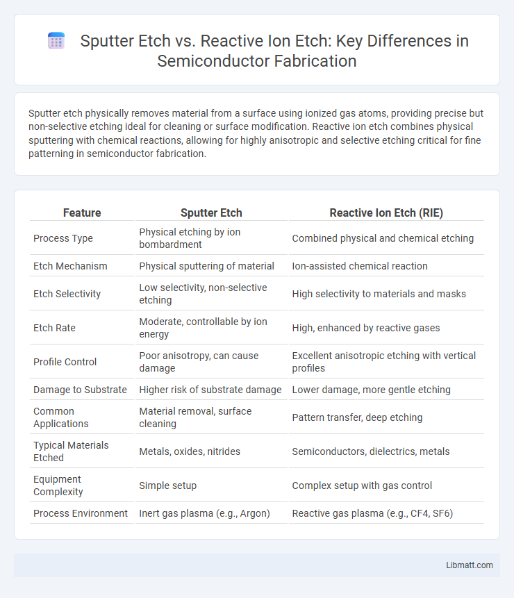
Sputter etch physically removes material from a surface using ionized gas atoms, providing precise but non-selective etching ideal for cleaning or surface modification. Reactive ion etch combines physical sputtering with chemical reactions, allowing for highly anisotropic and selective etching critical for fine patterning in semiconductor fabrication.
Table of Comparison
| Feature | Sputter Etch | Reactive Ion Etch (RIE) |
|---|---|---|
| Process Type | Physical etching by ion bombardment | Combined physical and chemical etching |
| Etch Mechanism | Physical sputtering of material | Ion-assisted chemical reaction |
| Etch Selectivity | Low selectivity, non-selective etching | High selectivity to materials and masks |
| Etch Rate | Moderate, controllable by ion energy | High, enhanced by reactive gases |
| Profile Control | Poor anisotropy, can cause damage | Excellent anisotropic etching with vertical profiles |
| Damage to Substrate | Higher risk of substrate damage | Lower damage, more gentle etching |
| Common Applications | Material removal, surface cleaning | Pattern transfer, deep etching |
| Typical Materials Etched | Metals, oxides, nitrides | Semiconductors, dielectrics, metals |
| Equipment Complexity | Simple setup | Complex setup with gas control |
| Process Environment | Inert gas plasma (e.g., Argon) | Reactive gas plasma (e.g., CF4, SF6) |
Introduction to Sputter Etch and Reactive Ion Etch
Sputter etch utilizes inert gas ions, typically argon, to physically remove material from a substrate through momentum transfer, enabling precise surface cleaning and pattern definition. Reactive ion etch combines physical ion bombardment with chemically reactive plasma species, enhancing etch anisotropy and selectivity for complex microfabrication processes. Both techniques are essential in semiconductor manufacturing for controlled material removal but differ in etch mechanisms and applications.
Fundamental Principles of Each Etching Method
Sputter etch operates by physically bombarding a substrate surface with high-energy ions, resulting in the ejection of atoms through momentum transfer, primarily relying on physical sputtering. Reactive ion etch (RIE) combines both physical sputtering and chemical reactions by using reactive plasma species to chemically modify and remove material in a more anisotropic fashion. The fundamental difference lies in sputter etch's dependence on inert ion bombardment versus RIE's synergy of ion energy and reactive gas chemistry to achieve controlled etching profiles.
Process Mechanisms: Physical vs. Chemical Etching
Sputter etching relies primarily on physical mechanisms, where high-energy ions bombard the surface to physically remove material via momentum transfer. Reactive ion etching (RIE) combines physical ion bombardment with chemical reactions, enabling selective material removal through reactive species that form volatile byproducts. The interplay of physical sputtering and chemical reactivity in RIE allows for enhanced anisotropy and etch rate control compared to purely physical sputter etching.
Equipment and Operational Differences
Sputter etch employs inert gas ions, typically argon, to physically remove material through ion bombardment, requiring simpler equipment with basic ion sources and no reactive gases. Reactive ion etch (RIE) combines physical sputtering with chemical reactions by using reactive gases like CF4 or SF6, necessitating more complex systems featuring plasma generators, gas flow controls, and RF power supplies. Operationally, sputter etching offers anisotropic etching with minimal chemical selectivity, while RIE provides greater precision and selectivity due to simultaneous physical and chemical etching mechanisms.
Advantages of Sputter Etch
Sputter etch offers superior surface cleaning and uniform material removal, making it ideal for precise substrate preparation. Its physical sputtering process provides excellent control over etch depth and minimal chemical contamination compared to reactive ion etch methods. This technique enhances feature definition in semiconductor fabrication, particularly for materials sensitive to chemical reactants.
Benefits of Reactive Ion Etch
Reactive Ion Etch (RIE) offers precise anisotropic etching, enabling high-resolution pattern transfer essential for microfabrication. It provides superior control over etch profiles and selectivity compared to sputter etch, minimizing damage to underlying layers. Your semiconductor or MEMS manufacturing process benefits from improved feature accuracy and consistency using RIE technology.
Key Applications in Microfabrication
Sputter Etch is primarily used for gentle surface cleaning and material removal in microfabrication, ideal for preparing substrates before thin film deposition or patterning. Reactive Ion Etch (RIE) offers high anisotropy and precise pattern transfer capabilities, making it essential for creating intricate semiconductor device features and deep trench structures. Your choice between sputter etch and RIE depends on the required etch profile control and material selectivity for microelectronic and MEMS fabrication processes.
Etch Rate, Selectivity, and Profile Comparison
Sputter etch typically exhibits a lower etch rate compared to reactive ion etch (RIE) due to its physical sputtering mechanism, which can be advantageous for precise material removal but slower in process throughput. RIE offers higher selectivity by combining chemical and physical etching, enabling more targeted removal of specific materials with reduced damage to underlying layers. Profile control in reactive ion etching generally yields anisotropic, vertical sidewalls essential for semiconductor fabrication, whereas sputter etching often produces more isotropic profiles, limiting its effectiveness for high-aspect-ratio structures.
Limitations and Challenges of Both Techniques
Sputter etch faces limitations such as poor selectivity and potential damage to underlying layers due to its physical sputtering process, which can lead to rough surfaces and substrate contamination. Reactive ion etch (RIE) offers better anisotropy and selectivity but struggles with issues like polymer buildup, etch rate non-uniformity, and potential damage from high-energy ions affecting delicate materials. Both techniques require precise control of process parameters to minimize defects, highlighting challenges in balancing etch rate, profile control, and substrate integrity for advanced microfabrication.
Choosing the Right Etching Process for Your Needs
Sputter Etch provides a physical sputtering method ideal for precise, low-damage material removal on delicate substrates, while Reactive Ion Etch (RIE) combines physical and chemical etching for high anisotropy and selective pattern transfer in microfabrication. Your choice depends on factors like etch rate, selectivity, substrate sensitivity, and feature resolution requirements. For applications demanding high precision with minimal chemical alteration, Sputter Etch is preferable, whereas RIE suits complex patterning needing directional etching and higher throughput.
Sputter Etch vs Reactive Ion Etch Infographic