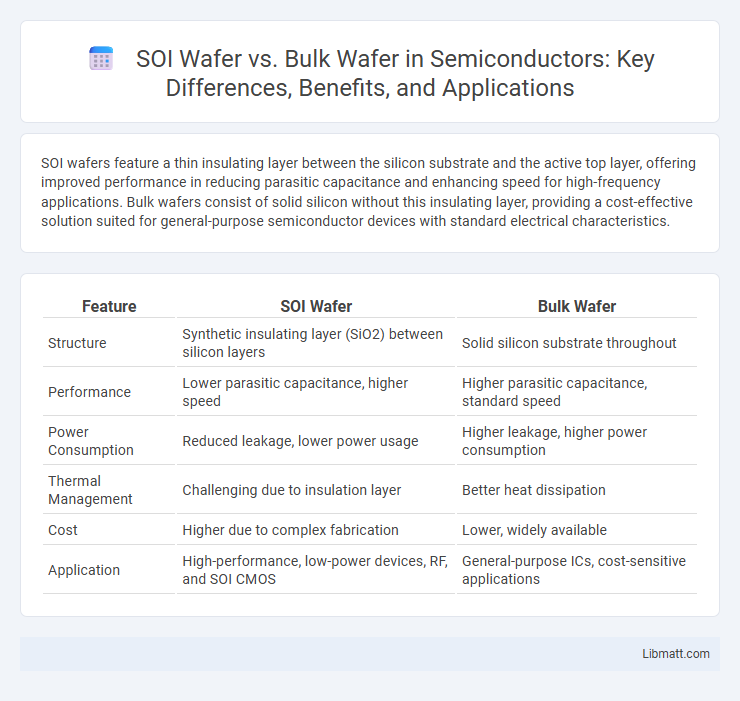
SOI wafers feature a thin insulating layer between the silicon substrate and the active top layer, offering improved performance in reducing parasitic capacitance and enhancing speed for high-frequency applications. Bulk wafers consist of solid silicon without this insulating layer, providing a cost-effective solution suited for general-purpose semiconductor devices with standard electrical characteristics.
Table of Comparison
| Feature | SOI Wafer | Bulk Wafer |
|---|---|---|
| Structure | Synthetic insulating layer (SiO2) between silicon layers | Solid silicon substrate throughout |
| Performance | Lower parasitic capacitance, higher speed | Higher parasitic capacitance, standard speed |
| Power Consumption | Reduced leakage, lower power usage | Higher leakage, higher power consumption |
| Thermal Management | Challenging due to insulation layer | Better heat dissipation |
| Cost | Higher due to complex fabrication | Lower, widely available |
| Application | High-performance, low-power devices, RF, and SOI CMOS | General-purpose ICs, cost-sensitive applications |
Introduction to SOI Wafer and Bulk Wafer
SOI wafers consist of a thin silicon layer separated from the substrate by an insulating oxide layer, enhancing performance by reducing parasitic capacitance and improving thermal efficiency. Bulk wafers are traditional silicon substrates without the buried oxide layer, widely used for general-purpose semiconductor manufacturing due to their cost-effectiveness and established processing techniques. Your choice between SOI and bulk wafers depends on the specific requirements for device performance, power consumption, and fabrication complexity.
What is an SOI Wafer?
An SOI wafer, or Silicon-On-Insulator wafer, consists of a thin layer of silicon separated from the bulk silicon substrate by a buried oxide layer, enhancing device performance by reducing parasitic capacitance and improving speed. Unlike bulk wafers, SOI wafers minimize leakage current and power consumption, making them ideal for high-performance and low-power semiconductor applications. The buried oxide layer in SOI wafers also provides superior isolation, which enhances device reliability and radiation resistance in advanced integrated circuits.
What is a Bulk Wafer?
A bulk wafer is a semiconductor substrate made from a single, solid piece of crystalline silicon, commonly used in traditional integrated circuit manufacturing. It offers cost-effective, high-purity material ideal for standard electronic devices but lacks the insulating layer found in SOI (Silicon-On-Insulator) wafers. Your choice between bulk and SOI wafers depends on factors like device performance, heat dissipation, and fabrication complexity.
Key Differences Between SOI and Bulk Wafers
SOI wafers consist of a thin silicon layer separated from the bulk substrate by an insulating oxide layer, resulting in reduced parasitic capacitance and improved performance in high-speed and low-power applications. Bulk wafers are made entirely of silicon, offering cost-effectiveness and mechanical robustness but higher leakage currents and slower switching speeds. Your choice between SOI and bulk wafers impacts device efficiency, power consumption, and overall integration complexity in semiconductor manufacturing.
Electrical Performance Comparison
SOI (Silicon on Insulator) wafers exhibit superior electrical performance compared to bulk wafers, offering reduced parasitic capacitance and improved isolation that enhances switching speeds and lowers power consumption in integrated circuits. The buried oxide layer in SOI wafers minimizes leakage currents, resulting in higher device reliability and better signal integrity, especially in high-frequency applications. Bulk wafers, while cost-effective, face challenges with increased junction capacitance and substrate noise coupling, which can degrade overall circuit performance.
Applications of SOI Wafers
SOI wafers are extensively used in high-performance microprocessors, RF applications, and low-power devices due to their excellent electrical isolation and reduced parasitic capacitance. Your designs benefit from improved speed, lower power consumption, and enhanced radiation hardness, making SOI wafers ideal for automotive, aerospace, and advanced sensor technologies. Unlike bulk wafers, SOI substrates provide superior thermal management and signal integrity in demanding environments.
Applications of Bulk Wafers
Bulk wafers are widely used in power electronics, sensors, and traditional CMOS circuits due to their cost-effectiveness and robustness. These wafers support high voltage and high current applications such as power MOSFETs, IGBTs, and solar cells, where thermal conductivity and substrate strength are critical. The bulk silicon substrate's compatibility with conventional fabrication processes makes it ideal for large-scale production of MEMS devices and analog integrated circuits.
Cost Considerations: SOI vs Bulk
SOI wafers generally have higher initial costs compared to bulk wafers due to complex manufacturing processes and specialized materials, such as the buried oxide layer. While bulk wafers offer lower upfront expenses, SOI wafers can reduce overall system costs by improving device performance, yield, and power efficiency in high-end applications. Cost-benefit analysis between SOI and bulk wafers depends on the specific use case, volume production, and required circuit characteristics.
Manufacturing Process Differences
SOI wafer manufacturing involves bonding a thin layer of silicon oxide between two silicon layers, utilizing techniques like wafer bonding and layer transfer, which helps reduce parasitic capacitance and improve device isolation. In contrast, bulk wafer production employs a simpler process of slicing and polishing a single silicon crystal, typically grown by the Czochralski method, resulting in a homogeneous silicon substrate. The complexity of SOI wafer fabrication increases production cost but offers superior electrical performance compared to bulk wafers.
Future Trends in SOI and Bulk Wafer Technologies
SOI wafer technology is advancing with trends toward ultra-thin layers and enhanced insulation for better performance in high-frequency and low-power applications, driving innovation in 5G and AI devices. Bulk wafer technology continues to evolve with improved purity and larger diameters, enabling cost-effective manufacturing for mainstream semiconductors in consumer electronics. Your choice between SOI and Bulk wafers will depend on the specific demands of future chip designs, balancing performance, power efficiency, and production volume.
SOI Wafer vs Bulk Wafer Infographic