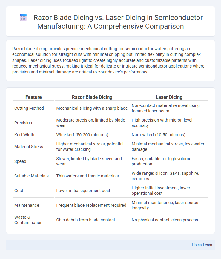
Razor blade dicing provides precise mechanical cutting for semiconductor wafers, offering an economical solution for straight cuts with minimal chipping but limited flexibility in cutting complex shapes. Laser dicing uses focused light to create highly accurate and customizable patterns with reduced mechanical stress, making it ideal for delicate or intricate semiconductor applications where precision and minimal damage are critical to Your device's performance.
Table of Comparison
| Feature | Razor Blade Dicing | Laser Dicing |
|---|---|---|
| Cutting Method | Mechanical slicing with a sharp blade | Non-contact material removal using focused laser beam |
| Precision | Moderate precision, limited by blade wear | High precision with micron-level accuracy |
| Kerf Width | Wide kerf (50-200 microns) | Narrow kerf (10-50 microns) |
| Material Stress | Higher mechanical stress, potential for wafer cracking | Minimal mechanical stress, less wafer damage |
| Speed | Slower, limited by blade speed and wear | Faster, suitable for high-volume production |
| Suitable Materials | Thin wafers and fragile materials | Wide range: silicon, GaAs, sapphire, ceramics |
| Cost | Lower initial equipment cost | Higher initial investment, lower operational cost |
| Maintenance | Frequent blade replacement required | Minimal maintenance; laser source longevity |
| Waste & Contamination | Chip debris from blade contact | No physical contact; clean process |
Introduction to Dicing Techniques
Razor blade dicing utilizes a mechanical blade to precisely cut semiconductor wafers into individual dies, offering high throughput and cost efficiency. Laser dicing employs a focused laser beam to ablate material, enabling minimal kerf loss and reduced mechanical stress on sensitive components. Understanding these dicing techniques helps optimize Your semiconductor manufacturing process by balancing precision, speed, and material integrity.
Overview of Razor Blade Dicing
Razor blade dicing employs a precision diamond-coated blade to mechanically cut semiconductor wafers into individual die, ensuring high throughput and low cost for silicon and glass substrates. This method provides minimal kerf loss with clean edge profiles, suitable for delicate chips requiring high-quality dicing. Razor blade dicing is favored for its simplicity and reduced thermal impact compared to laser dicing, making it an efficient choice for various microelectronic applications.
Overview of Laser Dicing
Laser dicing is a precision semiconductor cutting method that uses focused laser beams to scribe and separate wafers with minimal mechanical stress and high accuracy. This technique offers advantages such as reduced chipping, enhanced edge quality, and the ability to dice ultra-thin wafers or fragile materials that are challenging for traditional razor blade dicing. By enabling finer kerf widths and higher throughput, laser dicing improves overall production yield and wafer utilization in advanced semiconductor manufacturing.
Material Compatibility
Razor blade dicing offers excellent compatibility with brittle materials such as silicon and glass, minimizing mechanical stress during the cutting process. Laser dicing excels in processing a wider range of materials, including metals and advanced ceramics, due to its non-contact, precise energy application. Your choice between these methods depends on the material type and the required cut quality for optimal device performance.
Precision and Accuracy Comparison
Razor blade dicing offers high precision for cutting relatively simple geometries with minimal kerf width, but it may struggle with complex or delicate patterns due to mechanical stresses. Laser dicing provides superior accuracy and the ability to achieve intricate, non-linear cuts with micron-level precision, minimizing chipping and cracking in brittle materials like silicon. The choice between razor blade and laser dicing hinges on the required cutoff precision, material properties, and the complexity of the die layout.
Speed and Throughput Analysis
Laser dicing offers higher speed and throughput compared to razor blade dicing by enabling non-contact, precise cutting that reduces mechanical stress and minimizes wafer breakage. Razor blade dicing relies on slower, contact-based mechanical slicing, resulting in longer cycle times and lower overall throughput. Your choice impacts manufacturing efficiency, with laser dicing increasingly preferred for high-volume semiconductor production due to its superior speed and scalability.
Edge Quality and Yield
Razor blade dicing offers superior edge quality with minimal chipping and micro-cracks, resulting in higher yield rates for brittle materials like silicon wafers. Laser dicing, while faster and more flexible for intricate patterns, may introduce thermal damage and recast layers that can degrade edge integrity and reduce overall yield. Optimizing choice between razor blade and laser dicing depends on balancing edge smoothness requirements and throughput demands to maximize semiconductor device performance.
Cost Implications and Efficiency
Razor blade dicing offers a lower upfront cost and simpler setup compared to laser dicing, making it more cost-effective for small to medium production volumes. However, laser dicing provides higher precision and faster processing speeds, improving efficiency and reducing overall waste in high-volume manufacturing. Your choice depends on balancing initial investment against long-term efficiency gains.
Applications in Semiconductor Manufacturing
Razor blade dicing is commonly used for singulating standard silicon wafers with minimal edge damage, making it suitable for applications requiring cost-effective, bulk wafer processing. Laser dicing offers precise cutting with reduced mechanical stress, ideal for advanced semiconductor devices like MEMS, LEDs, and thin wafers that demand high accuracy and minimal kerf loss. Semiconductor manufacturers select between these methods based on device sensitivity, wafer thickness, and production volume to optimize yield and performance.
Choosing the Right Dicing Method
Choosing the right dicing method depends on factors such as material hardness, precision requirements, and production volume. Razor blade dicing offers cost-effective and fast processing for softer materials and larger chips, while laser dicing provides higher precision and minimal kerf width ideal for delicate or high-density semiconductor wafers. Your selection impacts overall yield, edge quality, and device performance, making it essential to match the dicing technology to your specific application needs.
Razor Blade Dicing vs Laser Dicing Infographic