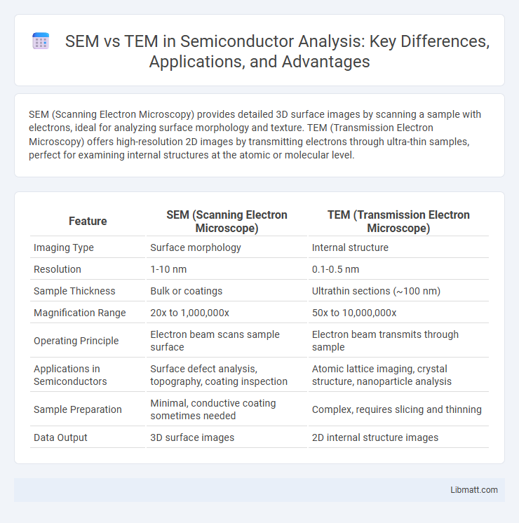
SEM (Scanning Electron Microscopy) provides detailed 3D surface images by scanning a sample with electrons, ideal for analyzing surface morphology and texture. TEM (Transmission Electron Microscopy) offers high-resolution 2D images by transmitting electrons through ultra-thin samples, perfect for examining internal structures at the atomic or molecular level.
Table of Comparison
| Feature | SEM (Scanning Electron Microscope) | TEM (Transmission Electron Microscope) |
|---|---|---|
| Imaging Type | Surface morphology | Internal structure |
| Resolution | 1-10 nm | 0.1-0.5 nm |
| Sample Thickness | Bulk or coatings | Ultrathin sections (~100 nm) |
| Magnification Range | 20x to 1,000,000x | 50x to 10,000,000x |
| Operating Principle | Electron beam scans sample surface | Electron beam transmits through sample |
| Applications in Semiconductors | Surface defect analysis, topography, coating inspection | Atomic lattice imaging, crystal structure, nanoparticle analysis |
| Sample Preparation | Minimal, conductive coating sometimes needed | Complex, requires slicing and thinning |
| Data Output | 3D surface images | 2D internal structure images |
Introduction to Electron Microscopy
Electron microscopy techniques like SEM (Scanning Electron Microscopy) and TEM (Transmission Electron Microscopy) provide detailed imaging at the nanoscale, essential for material science and biological research. SEM scans the surface with electrons to generate detailed 3D images, revealing texture and topography, while TEM transmits electrons through ultrathin samples to capture high-resolution internal structures. Understanding the differences between SEM and TEM helps optimize Your choice based on sample type, resolution needs, and analysis goals.
Overview of SEM and TEM
Scanning Electron Microscopy (SEM) utilizes a focused electron beam to scan the surface of a specimen, providing detailed three-dimensional images with high resolution and depth of field for surface morphology analysis. Transmission Electron Microscopy (TEM) transmits electrons through ultra-thin samples, offering atomic-level resolution to reveal internal structures and crystallography. Your choice between SEM and TEM depends on whether surface detail or internal composition analysis is required.
Working Principles: SEM vs TEM
Scanning Electron Microscopy (SEM) operates by scanning a focused electron beam across the specimen surface, detecting secondary and backscattered electrons to generate detailed topographical images. Transmission Electron Microscopy (TEM) transmits a high-energy electron beam through an ultra-thin specimen, capturing electrons that pass through to produce high-resolution internal structural images. SEM excels in surface morphology visualization, while TEM provides atomic to nanometer-scale internal structural detail by electron beam transmission.
Sample Preparation Techniques
SEM sample preparation techniques usually involve coating the specimen with a thin conductive layer like gold or carbon to prevent charging and improve image quality. TEM requires ultrathin sections, often less than 100 nanometers thick, achieved through microtomy or ion milling to allow electron transmission. Your choice between SEM and TEM hinges on the preparation complexity, with TEM demanding more precise and delicate sample handling.
Resolution and Magnification Differences
Scanning Electron Microscopy (SEM) offers resolution typically between 1 to 20 nanometers, with magnification ranging from 20x to around 1,000,000x, ideal for detailed surface imaging of samples. Transmission Electron Microscopy (TEM) provides significantly higher resolution, down to 0.1 nanometers, and magnification levels of up to 10,000,000x, enabling visualization of internal structures at the atomic level. The higher resolution and magnification capabilities of TEM make it indispensable for nanoscale material analysis, while SEM excels in providing three-dimensional surface morphology.
Imaging Modes and Contrast Mechanisms
SEM (Scanning Electron Microscopy) uses secondary and backscattered electrons for surface imaging, providing topographical and compositional contrast through electron-sample interactions. TEM (Transmission Electron Microscopy) transmits electrons through ultra-thin specimens, enabling imaging modes such as bright-field, dark-field, and high-resolution TEM, which reveal internal structures and crystallography with phase-contrast and diffraction contrast mechanisms. Your choice between SEM and TEM depends on whether surface morphology or internal nanoscale features are the primary focus of analysis.
Applications of SEM
Scanning Electron Microscopy (SEM) is widely utilized for detailed surface morphology analysis in materials science, electronics, and biological research. SEM's high-resolution imaging and large depth of field enable precise examination of microstructures, fractures, and coatings, making it essential for quality control and failure analysis. Your research benefits from SEM's ability to provide three-dimensional visualization and elemental composition through energy-dispersive X-ray spectroscopy (EDS).
Applications of TEM
Transmission Electron Microscopy (TEM) is essential for high-resolution imaging and detailed analysis of the internal structure of materials, making it invaluable in fields such as nanotechnology, materials science, and biology. TEM enables the examination of crystal structures, defects, and morphology at atomic or molecular scales, supporting research in semiconductor development and cellular biology. You can leverage TEM to investigate fine structural details that SEM cannot reveal, providing critical insights for advanced scientific and industrial applications.
Advantages and Limitations
Scanning Electron Microscopy (SEM) provides detailed surface topography and composition analysis with a larger depth of field, making it ideal for examining bulk materials and complex surfaces, while Transmission Electron Microscopy (TEM) delivers atomic-scale resolution and internal structure insights by transmitting electrons through ultrathin samples. SEM advantages include easier sample preparation and the ability to image larger samples, but it has lower resolution compared to TEM, which requires extensive sample preparation and operates under high vacuum conditions. Your choice depends on the need for surface detail from SEM or internal structural analysis at the nanoscale achievable with TEM.
Choosing Between SEM and TEM
Choosing between Scanning Electron Microscopy (SEM) and Transmission Electron Microscopy (TEM) depends primarily on the resolution and sample type needed. SEM provides detailed 3D images of surface morphology ideal for bulk materials and larger specimens, while TEM offers ultra-high resolution of internal structures at the atomic or molecular level, suitable for thin samples. Cost, sample preparation complexity, and analysis goals also influence the decision, with TEM demanding more specialized preparation and equipment investment.
SEM vs TEM Infographic