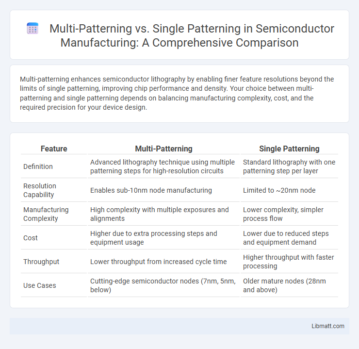
Multi-patterning enhances semiconductor lithography by enabling finer feature resolutions beyond the limits of single patterning, improving chip performance and density. Your choice between multi-patterning and single patterning depends on balancing manufacturing complexity, cost, and the required precision for your device design.
Table of Comparison
| Feature | Multi-Patterning | Single Patterning |
|---|---|---|
| Definition | Advanced lithography technique using multiple patterning steps for high-resolution circuits | Standard lithography with one patterning step per layer |
| Resolution Capability | Enables sub-10nm node manufacturing | Limited to ~20nm node |
| Manufacturing Complexity | High complexity with multiple exposures and alignments | Lower complexity, simpler process flow |
| Cost | Higher due to extra processing steps and equipment usage | Lower due to reduced steps and equipment demand |
| Throughput | Lower throughput from increased cycle time | Higher throughput with faster processing |
| Use Cases | Cutting-edge semiconductor nodes (7nm, 5nm, below) | Older mature nodes (28nm and above) |
Introduction to Lithography Patterning
Lithography patterning in semiconductor manufacturing defines critical device features using light to transfer circuit designs onto silicon wafers. Single patterning employs one exposure step per layer, limiting resolution to the wavelength and numerical aperture of the lithography system. Multi-patterning overcomes these limits by splitting complex patterns into multiple exposure and etch cycles, enabling smaller feature sizes and enhanced device density beyond the capabilities of single patterning.
What is Single Patterning?
Single Patterning is a photolithography technique in semiconductor manufacturing where a single exposure step defines the entire pattern on a wafer layer. This process is limited by the resolution of the lithography tool, typically effective for feature sizes above 20 nanometers. It contrasts with Multi-Patterning, which involves multiple exposure or etch steps to achieve finer feature sizes below the single exposure resolution limit.
What is Multi-Patterning?
Multi-patterning is a lithography technique used in semiconductor manufacturing to achieve smaller feature sizes beyond the resolution limits of single patterning. It involves multiple exposures or etching steps to define patterns on a wafer, enabling the creation of advanced nodes like 7nm and below. This method increases process complexity but allows continued scaling in chip fabrication where single patterning cannot meet the required density and precision.
Key Differences Between Multi-Patterning and Single Patterning
Multi-patterning employs multiple lithography steps to define complex semiconductor features beyond the resolution limits of single patterning, enabling finer node fabrication such as 7nm and below. Single patterning relies on a single lithography exposure, suitable for larger nodes like 28nm and above, but struggles with sub-20nm feature sizes due to diffraction limits. Key differences include process complexity, cost, overlay control, and achievable feature density, with multi-patterning significantly increasing manufacturing intricacy and expense to meet advanced technology node demands.
Advantages of Single Patterning
Single patterning offers simplified process control and reduced manufacturing complexity compared to multi-patterning, leading to lower defect rates and higher yield. It enables faster throughput by avoiding multiple lithography steps, which significantly cuts production time and cost. Your semiconductor fabrication benefits from a streamlined workflow and improved reliability with single patterning techniques.
Advantages of Multi-Patterning
Multi-patterning enables advanced semiconductor manufacturing by overcoming lithography resolution limits, allowing for finer feature sizes below the minimum pitch of single patterning. It enhances circuit density and improves device performance by enabling more precise patterning on silicon wafers. This technique also supports cost-effective scaling in technology nodes where traditional single patterning cannot achieve necessary feature dimensions.
Limitations and Challenges of Single Patterning
Single patterning faces significant limitations in achieving the extremely small feature sizes required for advanced semiconductor manufacturing, typically capping at around 10 nm. The challenges include increased photolithography complexity, resolution constraints, and higher costs due to the need for expensive extreme ultraviolet (EUV) lithography tools. Your ability to scale down devices is hindered, making multi-patterning techniques essential for overcoming these barriers and enabling finer feature definitions.
Limitations and Challenges of Multi-Patterning
Multi-patterning faces limitations such as increased process complexity and higher manufacturing costs compared to single patterning, requiring multiple lithography exposures and precise alignment to prevent defects. The challenges include managing overlay errors, increased pattern density constraints, and limited scalability beyond certain technology nodes like 7nm or 5nm. Your chip designs may encounter yield losses and longer production cycles due to these intricate multi-patterning steps.
Applications in Advanced Semiconductor Manufacturing
Multi-patterning techniques such as double patterning (DP) and quadruple patterning (QP) enable the fabrication of sub-7nm nodes by dividing complex lithography steps into multiple exposure cycles, overcoming the limitations of single patterning processes in advanced semiconductor manufacturing. Single patterning is limited to feature sizes above 20nm, while multi-patterning allows critical dimension scaling below the resolution of extreme ultraviolet (EUV) lithography, facilitating the production of high-density integrated circuits with increased transistor density and improved electrical performance. Applications in logic devices, high-performance microprocessors, and memory chips extensively utilize multi-patterning to achieve the required pattern fidelity and overlay control essential for cutting-edge process nodes.
Future Trends in Patterning Technology
Future trends in patterning technology emphasize the shift from single patterning to multi-patterning techniques to achieve smaller feature sizes below 7nm nodes in semiconductor manufacturing. Multi-patterning methods, such as double and quadruple patterning, enhance lithographic resolution and enable continued adherence to Moore's Law by overcoming limits of traditional single patterning processes. Advances like EUV lithography integration and directed self-assembly (DSA) are poised to complement multi-patterning, driving higher precision, lower costs, and scalability in next-generation chip fabrication.
Multi-Patterning vs Single Patterning Infographic