Ion implantation offers precise control over dopant concentration and depth, making it ideal for creating abrupt junctions in semiconductor devices, while diffusion relies on higher temperatures to introduce dopants over broader regions with less accuracy. Your choice between these techniques depends on desired device characteristics, processing temperature constraints, and fabrication complexity.
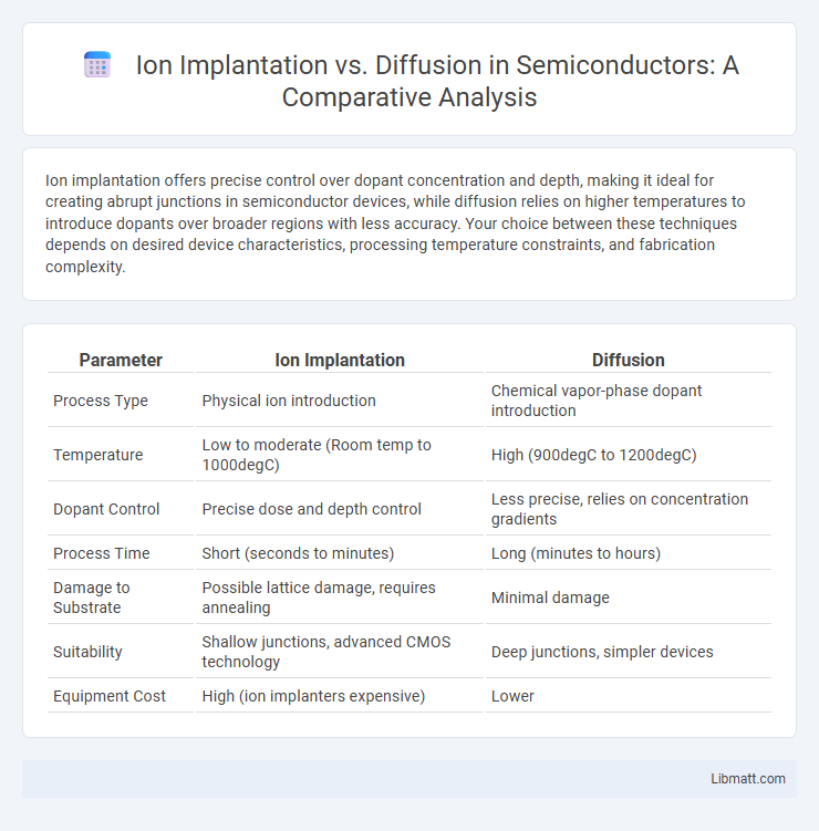
Table of Comparison
| Parameter | Ion Implantation | Diffusion |
|---|---|---|
| Process Type | Physical ion introduction | Chemical vapor-phase dopant introduction |
| Temperature | Low to moderate (Room temp to 1000degC) | High (900degC to 1200degC) |
| Dopant Control | Precise dose and depth control | Less precise, relies on concentration gradients |
| Process Time | Short (seconds to minutes) | Long (minutes to hours) |
| Damage to Substrate | Possible lattice damage, requires annealing | Minimal damage |
| Suitability | Shallow junctions, advanced CMOS technology | Deep junctions, simpler devices |
| Equipment Cost | High (ion implanters expensive) | Lower |
Introduction to Semiconductor Doping Techniques
Ion implantation and diffusion are fundamental semiconductor doping techniques essential for modifying electrical properties in silicon wafers. Ion implantation involves bombarding the semiconductor substrate with high-energy ions to introduce dopants precisely and with controlled depth profiles, enabling high-resolution patterning for advanced microelectronics. Diffusion relies on thermal processes to drive dopant atoms into the substrate, offering a cost-effective method but with less control over junction depth and doping concentration gradients compared to ion implantation.
Overview of Ion Implantation
Ion implantation is a precise semiconductor doping technique that introduces ions into the substrate by accelerating charged particles under high voltage. This method offers superior control over dopant depth and concentration profiles compared to traditional thermal diffusion, resulting in sharp junctions essential for modern integrated circuits. Understanding ion implantation helps optimize Your device performance by enabling tailored electrical properties at a micro-scale.
Fundamentals of Diffusion Doping
Diffusion doping involves introducing dopant atoms into a semiconductor substrate by heating it in the presence of a dopant source, allowing atoms to migrate and occupy lattice sites through thermal energy-driven concentration gradients. This process relies on Fick's laws of diffusion, where dopant concentration profiles develop over time depending on temperature and diffusion coefficients specific to the dopant-substrate pair. Unlike ion implantation, diffusion doping offers smoother dopant gradients but lacks precise control over depth and dose, making it essential for creating uniformly doped regions in silicon-based device fabrication.
Key Differences Between Ion Implantation and Diffusion
Ion implantation introduces dopants into a semiconductor substrate by bombarding it with high-energy ions, allowing precise control over dopant concentration and depth profiles, whereas diffusion relies on thermal energy to drive dopant atoms into the substrate from a gas or solid source, resulting in less sharp junctions. Ion implantation offers lower thermal budgets, reducing wafer damage and enabling shallow junction formation critical for modern integrated circuits. Your choice between ion implantation and diffusion affects device performance, manufacturing complexity, and scalability in semiconductor fabrication.
Process Steps of Ion Implantation
Ion implantation involves injecting high-energy ions directly into the semiconductor substrate, precisely controlling dopant concentration and depth by adjusting ion energy and dose. Post-implantation, annealing steps activate the dopants and repair crystal damage caused by ion bombardment. This process offers superior accuracy and uniformity compared to diffusion, which relies on high-temperature exposure to introduce dopants through thermal gradients.
Process Steps of Diffusion
Diffusion in semiconductor fabrication involves introducing dopant atoms into the wafer surface at high temperatures, where atoms move from high to low concentration regions based on Fick's laws. The process steps typically include drive-in diffusion, pre-deposition, and cleaning, requiring precise temperature control to ensure uniform dopant distribution and desired junction depth. Unlike ion implantation, diffusion relies on thermal energy for dopant incorporation, resulting in smoother junction profiles but less spatial precision.
Advantages and Disadvantages of Ion Implantation
Ion implantation offers precise control over dopant distribution and depth, enabling high uniformity and reduced thermal budget compared to diffusion. However, ion implantation can cause lattice damage requiring annealing for defect repair, and equipment costs are significantly higher than diffusion furnaces. Your semiconductor manufacturing process benefits from ion implantation's accuracy, but must account for potential crystal damage and increased operational expenses.
Advantages and Disadvantages of Diffusion
Diffusion offers a simple and cost-effective method for doping semiconductors, enabling uniform impurity distribution over large wafer areas. Its disadvantages include limited precision in controlling dopant depth and concentration, which can affect device performance. For your semiconductor fabrication needs, diffusion may suit applications where less exact doping profiles are acceptable.
Applications in Modern Semiconductor Manufacturing
Ion implantation enables precise doping of semiconductor substrates with controlled depth and concentration, making it ideal for fabricating advanced integrated circuits and nanoscale devices. Diffusion remains essential for forming uniform dopant profiles in regions requiring gradual concentration gradients, commonly used in older CMOS technologies and power devices. Combining ion implantation and diffusion allows manufacturers to optimize device performance, reliability, and scaling in modern semiconductor fabrication processes.
Choosing the Right Doping Method: Factors to Consider
Choosing the right doping method depends on factors such as precision, depth control, and wafer damage tolerance. Ion implantation offers superior accuracy and shallow junction profiling, making it ideal for advanced semiconductor devices requiring exact dopant placement. Your decision should also consider cost efficiency and thermal budget, as diffusion typically involves high-temperature processes that influence dopant distribution and overall device performance.
Ion Implantation vs Diffusion Infographic