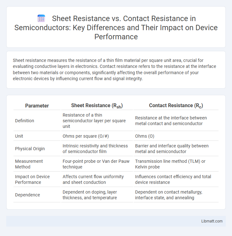
Sheet resistance measures the resistance of a thin film material per square unit area, crucial for evaluating conductive layers in electronics. Contact resistance refers to the resistance at the interface between two materials or components, significantly affecting the overall performance of your electronic devices by influencing current flow and signal integrity.
Table of Comparison
| Parameter | Sheet Resistance (Rsh) | Contact Resistance (Rc) |
|---|---|---|
| Definition | Resistance of a thin semiconductor layer per square unit | Resistance at the interface between metal contact and semiconductor |
| Unit | Ohms per square (O/#) | Ohms (O) |
| Physical Origin | Intrinsic resistivity and thickness of semiconductor film | Barrier and interface quality between metal and semiconductor |
| Measurement Method | Four-point probe or Van der Pauw technique | Transmission line method (TLM) or Kelvin probe |
| Impact on Device Performance | Affects current flow uniformity and sheet conduction | Influences contact efficiency and total device resistance |
| Dependence | Dependent on doping, layer thickness, and temperature | Dependent on contact metallurgy, interface state, and annealing |
Introduction to Sheet Resistance and Contact Resistance
Sheet resistance quantifies the resistance of a uniform thin film, typically measured in ohms per square, and plays a critical role in the performance of semiconductor devices and thin-film materials. Contact resistance refers to the resistance encountered at the interface between two conductive materials, significantly impacting current flow and device efficiency, especially in metal-semiconductor or metal-metal contacts. Understanding and minimizing both sheet resistance and contact resistance are essential for optimizing electrical conductivity and reliability in microelectronic and nanoelectronic applications.
Fundamental Concepts: Definitions and Differences
Sheet resistance quantifies the resistance of a thin film material per square unit, affecting current flow across its surface, typically measured in ohms per square (O/#). Contact resistance refers to the resistance at the interface where two conductive materials meet, impacting the efficiency of electrical signal transfer. The fundamental difference lies in sheet resistance relating to the intrinsic properties of the material layer, while contact resistance arises from interfacial phenomena such as surface roughness or contamination.
How Sheet Resistance is Measured
Sheet resistance is measured using the four-point probe method, which involves placing four equally spaced probes in contact with the material surface to accurately determine resistance without contact resistance interference. By sourcing current through the outer probes and measuring voltage across the inner probes, the sheet resistance can be calculated based on the voltage drop and current flow. Accurate measurement of your thin film or semiconductor materials' sheet resistance is critical for evaluating electrical performance and ensuring device reliability.
Understanding Contact Resistance in Electronic Devices
Contact resistance significantly affects the performance of electronic devices by impeding current flow at the interface between a metal contact and semiconductor material. Unlike sheet resistance, which measures resistance across a uniform thin film, contact resistance depends on factors such as interface quality, surface contamination, and the physical area of contact. Understanding and minimizing your device's contact resistance ensures improved conductivity, device efficiency, and overall reliability in electronic circuits.
Factors Affecting Sheet Resistance
Sheet resistance is influenced primarily by the thickness and resistivity of the material, with thinner films and higher resistivity increasing resistance values. Grain boundaries, impurities, and defects within the conductive layer also significantly affect sheet resistance by scattering charge carriers and impeding electron flow. Your device performance can be optimized by carefully controlling deposition methods and material quality to minimize these factors.
Variables Influencing Contact Resistance
Contact resistance is primarily influenced by factors such as the quality of the metal-semiconductor interface, surface roughness, and contamination layers that can create barriers to electron flow. The thickness and uniformity of the contact material, along with the doping concentration at the semiconductor contact region, significantly affect the ease of charge carrier injection. Temperature and pressure applied during contact formation further modify the microscopic contact area, directly impacting the contact resistance values.
Practical Applications: Where Sheet and Contact Resistance Matter
Sheet resistance is critical in thin-film applications such as solar cells, touchscreens, and flexible electronics where uniformity and low resistance per square impact device performance. Contact resistance plays a pivotal role in semiconductor devices and integrated circuits, affecting signal integrity and power efficiency at metal-semiconductor interfaces. Both resistances impact the reliability and speed of advanced electronic components, influencing design choices in microelectronics manufacturing.
Impact on Device Performance and Reliability
Sheet resistance determines the uniformity of current flow across semiconductor layers, directly influencing device speed and power consumption, while contact resistance affects the efficiency of charge transfer at metal-semiconductor interfaces, impacting overall device performance. High sheet resistance can lead to increased thermal dissipation and signal degradation, whereas elevated contact resistance can cause localized heating and reliability issues, such as electromigration and contact degradation over time. Optimizing both sheet and contact resistances is crucial for maintaining the performance, longevity, and reliability of your electronic devices.
Minimizing Sheet and Contact Resistance: Techniques and Best Practices
Minimizing sheet resistance involves optimizing material thickness, doping concentration, and uniformity to enhance conductivity in thin films, while contact resistance reduction relies on improving interface quality through surface cleaning, metallization techniques, and annealing processes. Techniques such as ion implantation, thermal treatments, and the use of low-resistivity metals like gold or silver effectively reduce resistance values, improving overall device performance. By carefully controlling fabrication parameters and ensuring proper contact formation, your electronic components can achieve lower resistance, enhancing efficiency and reliability.
Conclusion: Choosing the Right Parameter for Your Application
Selecting between sheet resistance and contact resistance depends on your device's performance priorities; sheet resistance indicates the uniformity and conductivity of thin films, while contact resistance measures the efficiency of electrical connections. For applications valuing overall material quality and current flow uniformity, low sheet resistance is critical. When optimizing interface contacts, minimizing contact resistance ensures better device reliability and reduced power loss.
Sheet Resistance vs Contact Resistance Infographic