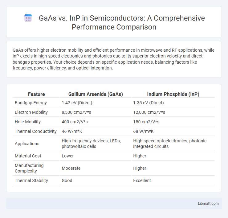
GaAs offers higher electron mobility and efficient performance in microwave and RF applications, while InP excels in high-speed electronics and photonics due to its superior electron velocity and direct bandgap properties. Your choice depends on specific application needs, balancing factors like frequency, power efficiency, and optical integration.
Table of Comparison
| Feature | Gallium Arsenide (GaAs) | Indium Phosphide (InP) |
|---|---|---|
| Bandgap Energy | 1.42 eV (Direct) | 1.35 eV (Direct) |
| Electron Mobility | 8,500 cm2/V*s | 12,000 cm2/V*s |
| Hole Mobility | 400 cm2/V*s | 150 cm2/V*s |
| Thermal Conductivity | 46 W/m*K | 68 W/m*K |
| Applications | High-frequency devices, LEDs, photovoltaic cells | High-speed optoelectronics, photonic integrated circuits |
| Material Cost | Lower | Higher |
| Manufacturing Complexity | Moderate | Higher |
| Thermal Stability | Good | Excellent |
Introduction to GaAs and InP
Gallium Arsenide (GaAs) and Indium Phosphide (InP) are prominent compound semiconductors widely used in high-frequency and optoelectronic applications due to their superior electron mobility compared to silicon. GaAs features a direct bandgap of 1.42 eV, ideal for infrared light emission and high-speed electronic devices, while InP boasts a direct bandgap of 1.34 eV, making it especially suited for photonic and high-frequency integrated circuits. Both materials underpin critical advancements in telecommunications, including laser diodes, photodetectors, and high-electron-mobility transistors (HEMTs).
Material Properties Comparison
Gallium Arsenide (GaAs) exhibits a direct bandgap of approximately 1.42 eV, high electron mobility around 8,500 cm2/V*s, and a lattice constant of 5.65 A, making it suitable for high-frequency and optoelectronic applications. Indium Phosphide (InP) offers a slightly larger direct bandgap of 1.34 eV, superior electron mobility near 12,000 cm2/V*s, and a lattice constant of 5.87 A, enabling better performance in photonic and high-speed electronic devices. Thermal conductivity is higher in InP (~68 W/m*K) compared to GaAs (~46 W/m*K), influencing device thermal management efficiency.
Bandgap and Electronic Characteristics
Gallium Arsenide (GaAs) features a direct bandgap of about 1.42 eV, enabling efficient electron-hole recombination ideal for optoelectronic devices such as LEDs and high-speed transistors. Indium Phosphide (InP) possesses a slightly larger direct bandgap of approximately 1.34 eV, offering superior electron mobility and higher saturation velocity, which benefits high-frequency and high-power applications. The electron mobility in InP surpasses GaAs, making InP devices preferable for radio frequency and photonic integrated circuits requiring faster electronic response.
Performance in High-Frequency Applications
Gallium arsenide (GaAs) exhibits superior electron mobility and high electron saturation velocity, making it highly effective for high-frequency applications such as microwave and millimeter-wave devices. Indium phosphide (InP) outperforms GaAs in ultra-high-frequency applications due to its higher electron velocity and better noise performance, which is critical in photonic and RF communication technologies. Both materials are preferred in high-frequency integrated circuits, with InP favored for faster, lower-noise transistors and GaAs for cost-effective RF power amplifiers.
Optical Properties and Photonics Use
Gallium Arsenide (GaAs) exhibits a direct bandgap of about 1.42 eV, making it highly efficient for emitting and detecting light in the near-infrared to visible spectrum, which facilitates its extensive use in LEDs, laser diodes, and photodetectors. Indium Phosphide (InP), with a direct bandgap of approximately 1.35 eV, is widely favored in photonics for high-speed optical communication due to its superior electron mobility and better lattice matching with InGaAs, enabling efficient integration in laser sources and photonic integrated circuits operating at wavelengths around 1.3 to 1.55 mm. GaAs is optimal for devices requiring high-frequency operation and visible to near-infrared photonics, while InP dominates fiber-optic telecommunication systems due to its material characteristics suited for long-wavelength infrared applications.
Device Integration and Fabrication
GaAs (Gallium Arsenide) supports mature device integration with well-established fabrication processes suitable for high-frequency and optoelectronic devices. InP (Indium Phosphide) offers superior electron velocity and integrates more efficiently with high-speed photonic components, making it preferable for integrated photonics and advanced communication systems. Fabrication on InP substrates poses challenges due to material brittleness and cost but enables direct integration of laser sources and detectors.
Cost and Availability of Materials
Gallium Arsenide (GaAs) is generally more affordable and widely available than Indium Phosphide (InP) due to its more established production infrastructure and lower raw material costs. InP substrates are rarer and more expensive because of the limited global supply of indium and the complexity involved in its purification and crystal growth processes. The higher cost and lower availability of InP materials often restrict its use to high-performance applications where its superior electronic and photonic properties justify the expense.
Reliability and Thermal Stability
Gallium Arsenide (GaAs) and Indium Phosphide (InP) exhibit distinct reliability and thermal stability profiles critical for high-performance applications. GaAs offers robust thermal stability up to approximately 250degC, making it suitable for devices operating in moderately high temperatures, while InP sustains stability beyond 300degC, providing superior reliability under extreme thermal conditions. Your choice between GaAs and InP should consider these temperature thresholds to ensure optimal device longevity and performance in demanding environments.
Popular Applications and Industries
Gallium Arsenide (GaAs) is widely used in high-frequency applications such as microwave and millimeter-wave circuits, including RF amplifiers and satellite communications, due to its high electron mobility and direct bandgap. Indium Phosphide (InP) finds extensive application in optical fiber communications and photonics, leveraging its superior electron velocity and efficient light emission properties for lasers and photodetectors. Your choice between GaAs and InP depends on whether your project prioritizes high-frequency RF performance or optoelectronic integration in telecommunications.
Future Trends in GaAs and InP Technologies
Future trends in GaAs and InP technologies emphasize advancements in high-frequency and high-speed applications, with GaAs continuing to dominate RF power amplifiers and InP leading in optical communication components. Enhanced material quality and novel fabrication techniques are driving improvements in device performance, such as higher electron mobility and superior thermal conductivity, critical for 5G and beyond. Your choice between GaAs and InP will depend on the specific requirements for speed, integration, and cost-efficiency in emerging semiconductor applications.
GaAs vs InP Infographic