Critical dimension (CD) defines the precise measurement of features on a semiconductor wafer, directly impacting device performance and yield. Overlay controls the accurate alignment of successive lithography layers, ensuring Your circuit patterns stack correctly for optimal functionality.
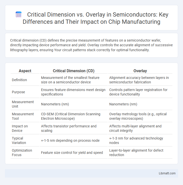
Table of Comparison
| Aspect | Critical Dimension (CD) | Overlay |
|---|---|---|
| Definition | Measurement of the smallest feature size on a semiconductor device | Alignment accuracy between layers in semiconductor fabrication |
| Purpose | Ensures feature dimensions meet design specifications | Controls pattern layer registration for device functionality |
| Measurement Unit | Nanometers (nm) | Nanometers (nm) |
| Measurement Tool | CD-SEM (Critical Dimension Scanning Electron Microscope) | Overlay metrology tools (e.g., optical overlay microscopes) |
| Impact on Device | Affects transistor performance and scaling | Affects multi-layer alignment and circuit integrity |
| Typical Variation | +-1-5 nm depending on process node | +-1-3 nm for advanced technology nodes |
| Optimization Focus | Feature size control for yield and speed | Layer-to-layer alignment for defect reduction |
Understanding Critical Dimension: Definition and Importance
Critical Dimension (CD) refers to the precise measurement of a feature's width or spacing on a semiconductor wafer, essential for ensuring device functionality and performance. Accurate control of CD impacts yield, device speed, and power consumption, making it a fundamental parameter in photolithography and process control. Understanding Critical Dimension helps you optimize manufacturing processes to achieve consistent, high-quality integrated circuits.
Overlay in Semiconductor Manufacturing Explained
Overlay in semiconductor manufacturing refers to the precise alignment between successive photolithography layers, critical for ensuring device performance and yield. Critical dimension (CD) defines the smallest feature size on a wafer, but overlay errors can cause misalignment, leading to defects despite accurate CD control. Advanced metrology tools measure overlay with nanometer accuracy to optimize layer stacking and minimize wafer rejection rates.
Key Differences Between Critical Dimension and Overlay
Critical Dimension (CD) refers to the precise measurement of specific features on a semiconductor wafer, such as line widths or spaces, ensuring device functionality. Overlay measures the alignment accuracy between multiple lithographic layers, crucial for layer-to-layer registration and preventing defects. Understanding the difference between CD's focus on feature size and overlay's focus on positional accuracy helps optimize your wafer manufacturing process for higher yield and performance.
Impact of Critical Dimension on Device Performance
Critical dimension (CD) directly affects transistor switching speed and power consumption by determining gate length and width precision in semiconductor devices. Variations in CD can cause significant performance degradation, such as increased leakage current and reduced drive current, impacting overall device efficiency. Ensuring tight CD control during lithography and etching processes is essential for optimizing your device performance and yield.
Overlay Control: Ensuring Alignment Accuracy
Overlay control is essential for maintaining alignment accuracy between successive photolithography layers, directly impacting device performance and yield in semiconductor manufacturing. Precise overlay measurement techniques, such as advanced metrology tools using scatterometry or image-based methods, enable detection of nanoscale misalignments. Ensuring your process employs rigorous overlay control minimizes defects and supports critical dimension (CD) uniformity across wafers, optimizing overall chip functionality.
Measurement Techniques for Critical Dimension
Critical dimension measurement techniques primarily employ scanning electron microscopy (SEM) for high-resolution imaging of nanoscale features, enabling precise linewidth and spacing analysis. Optical critical dimension (OCD) metrology uses spectroscopic reflectometry to determine feature dimensions non-destructively through light scattering patterns. Atomic force microscopy (AFM) provides three-dimensional surface topology for critical dimension verification, complementing SEM and OCD in semiconductor manufacturing.
Advanced Methods for Overlay Metrology
Advanced methods for overlay metrology employ techniques such as scatterometry and in-die metrology to accurately measure critical dimension variations and overlay errors at the nanoscale. These methods enhance alignment precision by analyzing diffraction patterns and leveraging machine learning algorithms, ensuring tighter control of layer-to-layer positioning in semiconductor manufacturing. Your manufacturing yield and device performance significantly benefit from the increased accuracy and speed provided by these state-of-the-art overlay metrology solutions.
Common Challenges in Critical Dimension and Overlay Control
Common challenges in Critical Dimension (CD) and Overlay control include measurement accuracy and process variability, which directly impact semiconductor yield and device performance. Maintaining strict control over CD uniformity and overlay alignment requires advanced metrology tools and robust statistical process control (SPC) methods. Your ability to address these challenges ensures tighter process windows and improved wafer-to-wafer consistency in semiconductor manufacturing.
Role of CD and Overlay in Yield Optimization
Critical Dimension (CD) controls the precise measurements of semiconductor features, directly impacting device performance and electrical characteristics. Overlay accuracy ensures proper alignment between successive lithography layers, minimizing pattern misregistration that can cause defects. Together, optimized CD and overlay reduce process variability, enhancing yield by preventing circuit failures and improving overall manufacturing reliability.
Future Trends in CD and Overlay Technology
Future trends in Critical Dimension (CD) and Overlay technology emphasize increased precision through AI-driven metrology and real-time process adjustments to meet shrinking semiconductor nodes. Advanced optical and electron-beam inspection tools enhance overlay accuracy, supporting complex 3D architectures and multi-layer designs. Your semiconductor production will benefit from these innovations by achieving tighter tolerances and improved yield efficiency.
Critical Dimension vs Overlay Infographic